Features
● VIN1 input voltage range: 0.6V to 2.2V
● DVDD1/2 output voltage range: 0.6V~1.8V
● DVDD1/2 dropout voltage: 135mV(IOUT=1.2A, 1.2V output)
● DVDD1/2 output drive capability: 1.2A(Typ.) The max of DVDD1/2 output drive capability can be set to 1.5A by config I2C
● VIN2 input voltage range: 2.5V to 5.5V
● AVDD1/2 output voltage range: 1.2V~4.3V
● AVDD1/2 dropout voltage: 125mV (IOUT=400mA , VOUT=2.8V)
● AVDD1/2 output drive capability: 400mA(Typ.) The max of AVDD1/2 output drive capability can be set to 600mA by config I2C
● AVDD1/2 power supply rejection ratio: typical 94dB (IOUT=50mA, 2.8V output, freq=1kHz)
● AVDD1/2 noise: typical 9µVrms (IOUT=30mA, BW=10Hz to 100KHz)
● Quiescent current: typical: 65µA
● Shutdown current: typical: 0.75µA
● Available with 1.2V I/O
● Build in 1.9V falling UVLO protection
● Build in OCP, SCP,OTP protection
● Programmable I²C Address
● DFN 2mm × 2mm × 0.75mm-10L package
Description
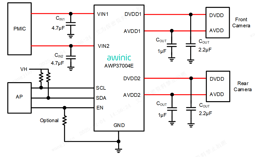
AWP37004EDNR is a 4-ch integrated LDO PMIC for camera applications include 2-ch DVDD, 2-ch AVDD, with 1MHz high speed I2C interface, the function setting is flexible such as power sequence, output discharge. The chip enable control support EN pin control and I2C control.
Due to high load current and lower working voltage of DVDD, AWP37004EDNR used N-MOSFET LDO architecture without charge pump for 2-ch DVDD LDO. DVDD LDO input source is VIN1 and VIN2 is the bias voltage. Ultra-low dropout voltage of DVDD LDOs is designed for high efficiency and lower power dissipation purpose.
For the AVDD, AWP37004EDNR used P-MOSFET LDO architecture. The input source is VIN2. Due to high performance requirement of AVDD, AWP37004EDNR’s AVDD used special circuit design and optimized pin assignment which is easy for system PCB layout.