

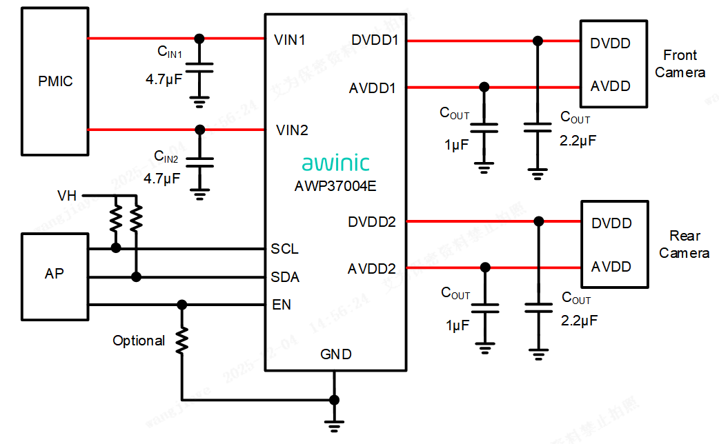
| Load Current (mA) | DVDD:1.5A AVDD:0.6A |
| Channel | 4 |
| Power Supply (Min) (V) | VIN1:0.6 VIN2:2.5 |
| Power Supply (Max) (V) | VIN1:2.2 VIN2:5.5 |
| Vout (V) | DVDD:0.6~1.8 AVDD:1.2~4.3 |
| Vdropout (mV) | DVDD:135@1.2A AVDD:125@0.4A |
| Iq (Typ) (μA) | 65 |
| PSRR @1KHz(dB) | DVDD:76@10mA AVDD:94@50mA |
| Output Noise (μVrms) | DVDD:90@30mA AVDD:9@30mA |
| Discharge | Programmable |
| Output options | Programmable |
| Temperature | -40℃~85℃ |
| IO Level (V) | 1.2 |
| Package (mm) | DFN 2X2-10L |
| DFN 2X2-10L |
|
タイプ
|
タイトル
|
言語
|
日付 | |||
|---|---|---|---|---|---|---|
| Datasheet | DS_AWP37004E_EN_V1.2 | 英文 | 2026-04-29 | |||
| Reliability Report | Reliability Qualification Report For AWP37004EDNR | 英文 | 2026-05-19 |
評価ボード
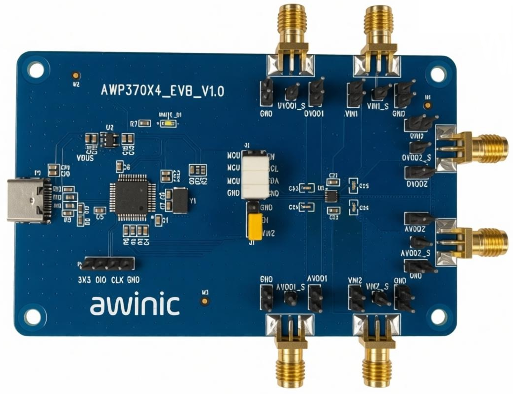
AWP370X4_EVB_V1.0 — AWP370X4_EVB_V1.0 is a 4-ch integrated LDO PMIC test board,include 2-ch DVDD, 2-ch AVDD, the main test points of the chip are drawn separately on the EVB board for convenient testing.
Evaluation board for the 4-in-1 LDO PMIC AWP370X4

APPLICATION SOFTWARE&FRAMEWORK
AWP37004_GUI — AWP37004 product tuning GUI plugin
AWP37004 product tuning GUI plugin. Requires AwinicSCPV4 installed.
DRIVER OR LIBRARY
AWP370X4_Driver — Android and other drivers for AWP370X4 series
Android and other drivers for AWP370X4 series,including sample code,configuration files,porting guide,etc
APPLICATION SOFTWARE&FRAMEWORK
AwinicSCPV4_GUI — AwinicSCPV4 Intelligent Tuning Tool
AwinicSCPV4 is an intelligent tuning tool specifically designed for Awinic products, facilitating product configuration and debugging processes. Intuitive interface and user-friendly operation can help customers shorten development time and complete system integration quickly.

評価ボード
AWP370X4_EVB_V1.0 — AWP370X4_EVB_V1.0 is a 4-ch integrated LDO PMIC test board,include 2-ch DVDD, 2-ch AVDD, the main test points of the chip are drawn separately on the EVB board for convenient testing.
Evaluation board for the 4-in-1 LDO PMIC AWP370X4
APPLICATION SOFTWARE&FRAMEWORK
AWP37004_GUI — AWP37004 product tuning GUI plugin
AWP37004 product tuning GUI plugin. Requires AwinicSCPV4 installed.
DRIVER OR LIBRARY
AWP370X4_Driver — Android and other drivers for AWP370X4 series
Android and other drivers for AWP370X4 series,including sample code,configuration files,porting guide,etc
APPLICATION SOFTWARE&FRAMEWORK
AwinicSCPV4_GUI — AwinicSCPV4 Intelligent Tuning Tool
AwinicSCPV4 is an intelligent tuning tool specifically designed for Awinic products, facilitating product configuration and debugging processes. Intuitive interface and user-friendly operation can help customers shorten development time and complete system integration quickly.


沪ICP备10011954号 |

沪公网安备 31011202011955号
