Features
VIN1 input voltage range: 0.6V to 2.2V
DVDD1/2 output voltage range: 0.6V~1.8V
DVDD1/2 dropout voltage: 90mV@1A
DVDD1/2 output drive capability: 1.5A(Typ.)
The output drive capability of DVDD1 can be set by config I2C
VIN2 input voltage range: 2.3V to 5.5V
VIN3 input voltage range: 1.8V to 5.5V
AVDD1/2/3 output voltage range: 1.2V~4.3V
AVDD1/2/3 dropout voltage: 60mV@300mA
AVDD1/2/3 output drive capability: 400mA(Typ.)
The max of AVDD1/2/3 output drive capability can be set to 600mA by config I2C
AVDD1/2/3 power supply rejection ratio: typical 96dB (IOUT=100mA, Freq=1kHz)
AVDD1/2/3 noise: typical 9µVrms (IOUT=30mA, BW=10Hz to 100kHz)
Quiescent current: typical: 100µA
Shutdown current: typical: 0.9µA
WLCSP 1.083mm×1.474mm×0.38mm-12B package
Description
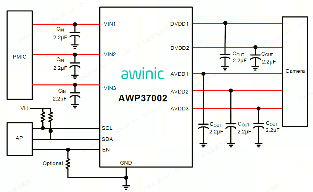
AWP37002CSR is a 5-ch integrated LDO PMIC for camera applications include 2-ch DVDD, 3-ch AVDD, with 1MHz high speed I2C interface, the function setting is flexible such as power sequence, output discharge. The chip can be enabled by I2C.
Due to high load current and lower working voltage of DVDD, AWP37002 used N-MOSFET LDO architecture without charge pump for 2-ch DVDD LDO, for the AVDD, AWP37002 used P-MOSFET LDO architecture. VIN2 serves as the system power supply, providing power to the internal fundamental modules and simultaneously supplying AVDD1 and AVDD2. VIN1 is the power supply for DVDD1 and DVDD2, while VIN3 is the power supply for AVDD3.
AWP37002 is designed to work with a 2.2µF or more input ceramic capacitor and a 2.2µF or more output ceramic capacitor. The low power dissipation and good dynamic response make AWP37002 very suitable for hand-held communication equipment. Tiny package makes high density mounting of the IC on boards possible.