Features
AEC-Q100 Qualified With Following Results:
- Device Operating Temperature Grade 1:
-40°C to +125°C
- Device HBM ESD Classification: Class 3A
- Device CDM ESD Classification: Class C3
1.2V~3.6V on A Port and 1.65V~5.5V on B Port(VCCA ≤ VCCB)
Maximum Data Rates:100Mbps(Push Pull)
This Device Can Only Translate Push-pull CMOS Logic Outputs
No Direction-Control Signal Required
Qualified for Automotive Applications
VCC Isolation Feature – If Either VCC Input is at GND, All Output are in the High-Impedance State
OE Input Circuit Referenced to VCCA
Support Ultra-Low Power Consumption Mode with OE Pin is Low Voltage Level
ESD Protection Exceeds AEC-Q100
A Port:
- 4KV Human-Body Model (ANSI/ESDA/JEDEC JS-001-2023)
- 1KV Charged-Device Model (ANSI/ESDA/JEDEC JS-002-2022)
B Port:
- 15KV Human-Body Model (ANSI/ESDA/JEDEC JS-001-2023)
- 1KV Charged-Device Model (ANSI/ESDA/JEDEC JS-002-2022)
Description
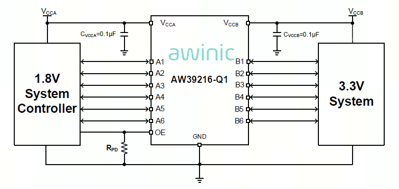
AW39216-Q1 is a 6-bit high-performance voltage-level translator without direction control signal, that enables bidirectional voltage level translation. It features two 6-bit input-output ports (An and Bn), one output enable input (OE) and two supply pins (VCCA and VCCB). VCCA can be supplied with any voltage between 1.2V and 3.6V. VCCB can be supplied with any voltage between 1.65V and 5.5V. The range of supply voltages makes the device suitable for translating between any of the low voltage nodes (1.2V, 1.5V, 1.8V, 2.5V, 3.3V and
5.0V).
The AW39216-Q1 is designed so that the OE input circuit is supplied by VCCA. When the output-enable (OE) input is low, all outputs are placed in the high-impedance state. To ensure the high-impedance state during power up or power down, OE should be tied to GND through a pulldown resistor; the minimum value of the resistor is determined by the current-sourcing capability of the driver.
This product has been qualified to the Automotive Electronics Council (AEC) standard Q100 (Grade1) and is suitable for use in automotive applications.