

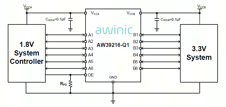
| Data Rate (Max) (Mbps) | 100 |
| VCCA (Min) (V) | 1.2 |
| VCCA (Max) (V) | 3.6 |
| VCCB (Min) (V) | 1.65 |
| VCCB (Max) (V) | 5.5 |
| ICCA+ICCB (Max) (μA) | 30 |
| Channel | 6 |
| Support | Push-Pull |
| Temperature | -40℃~125℃ |
| Transmission Direction | Auto |
| Package (mm) | TSSOP-16L |
| WBTSSOP-16L(1.2) |
|
유형
|
제목
|
언어
|
날짜 | |||
|---|---|---|---|---|---|---|
| Product Design Guide | AW39216-Q1 硬件设计指南 | 中文 | 2024-04-11 | |||
| Datasheet | DS_AW39216-Q1_EN_V1.0 | 英文 | 2024-11-12 |
평가 보드
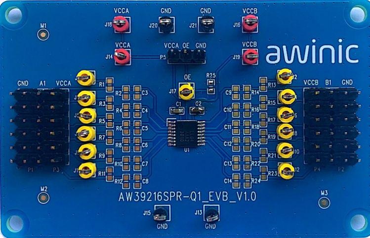
AW39216SPR-Q1_EVB_V1.0 — AW39216SR-Q1_EVB_V1.0 is a six channel adaptive bidirectional level converter test board from AWINIC.
This EVB is an evaluation board suitable for six channel level conversion chips

평가 보드
AW39216SPR-Q1_EVB_V1.0 — AW39216SR-Q1_EVB_V1.0 is a six channel adaptive bidirectional level converter test board from AWINIC.
This EVB is an evaluation board suitable for six channel level conversion chips


沪ICP备10011954号 |

沪公网安备 31011202011955号
