Features
AEC-Q100 in Progress
Broadband frequency range: 0.1 to 5.925GHz
Wide VDD range: 1.65V to 3.3V
GPIO interface for 1.0V to VDD positive control
voltage
Low insertion loss: 0.35dB typical @ 2.7GHz
Max input RF power of 38.5dBm
Excellent linearity and harmonic performance
No DC blocking capacitors in typical application
Small QFN 1.5X1.1-10L package
Description
The AW12022TQNR-Q1 is a Silicon-On-Insulator(SOI) DPDT switch with low insertion loss and high Isolation. It can be used to support band switching and mode switching for cellular 4G/5G, data cards and tablets.
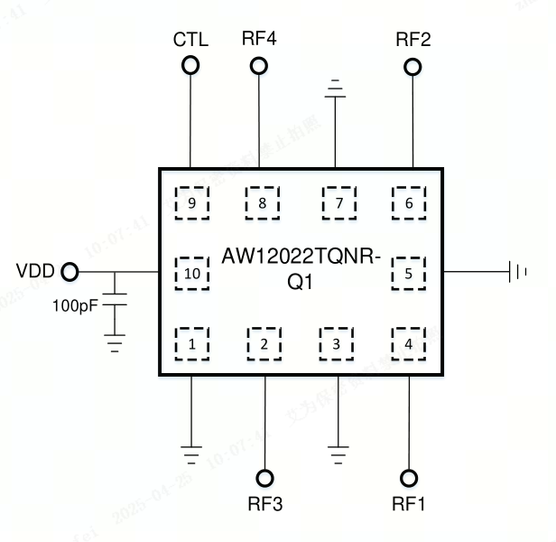
The symmetrical design of internal ports makes it convenient for PCB routing and adjustment of receiving and transmitting signals. The band/mode switching is realized by the GPIO pin as referenced in the chip block diagram and the control logic. The chip allows power-supply voltages from 1.65V to 3.3V and the positive control voltages from 1.0V to VDD.
The AW12022TQNR-Q1 is provided in a compact QFN 1.5X1.1-10L package.