EN

AW12022TQNR

0.1-6GHz DPDT Antenna Cross Switch

Product details

Parameters

Frequency (GHz) 0.1~6
Switch Feature DPDT Antenna
Control Interface GPIO
VDD (Min) (V) 1.65
VDD (Max) (V) 3.3
VIO (Min) (V) /
VIO (Max) (V) /
P0.1dB (dBm) 39
IL (Min) (dB) 0.29
IL (Max) (dB) 0.39
ISO (Max) (dB) 33
ISO (Min) (dB) 30
Temperature -40℃~85℃
Package (mm) QFN 1.5X1.1-10L

Package | Pins | Size

QFN 1.5X1.1-10L

Features

• Broadband frequency range: 0.1 to 6.0GHz
• Wide VDD range: 1.65V to 3.3V
• GPIO interface for 1.0V to VDD positive control voltage
• Low insertion loss: 0.41dB typical @ 2.7GHz
• Max input RF power of 39dBm
• Excellent linearity and harmonic performance
• No DC blocking capacitors in typical application
• Small WBQFN (1.5mm x 1.1mm x 0.45mm -10L) package

Description

The AW12022TQNR is a Silicon-On-Insulator(SOI) DPDT switch with low insertion loss and high Isolation. It can be used to support band switching and mode switching for cellular 4G/5G, data cards and tablets.
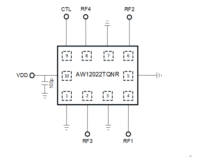
The symmetrical design of internal ports makes it convenient for PCB routing and adjustment of receiving and transmitting signals. The band/mode switching is realized by the GPIO pin as referenced in the chip block diagram and the control logic. The chip allows power-supply voltages from 1.65V to 3.3V and the positive control voltages from 1.0V to VDD.
The AW12022TQNR is provided in a compact WBQFN 1.5mm x 1.1mm x 0.45mm -10L package.

Technical documentation

Type
Title
Language
Date
Datasheet DS_AW12022TQNR_6GHz_DPDT_EN_V1.1 英文   2023-06-06

Design & development

For additional terms or required resources, click any title below to view the detail page where available.