EN

AWS74LVC1G17STR

Single Schmitt-Trigger Buffer

Product details

Parameters

Logic Type Noninverting Buffers
Power Supply (Min) (V) 1.65
Power Supply (Max) (V) 5.5
Channel 1
Data Rate (Max) (Mbps) /
ICCA+ICCB (Max) (μA) 1
Temperature -40℃~125℃
Tpd (Typ) (ns) 3.7@3.3V
Package (mm) WBSOT353-5L(1.1)
Output Type
IOLmax (Max) (mA) 32
IOHmax (Max) (mA) 32

Package | Pins | Size

WBSOT353-5L(1.1)

Features

Wide Supply Voltage Range: 1.65 V to 5.5 V CMOS Low Power Consumption Input Accept Voltage to 5.5 V IOFF Supports Partial Power-Down-Mode Operation tpd = 3.7 ns at 3.3 V High Output Drive: ±24 mA at VCC = 3.0 V Operating Temperature Range:-40 °C to 125 °C SOT353 - 5L

Description

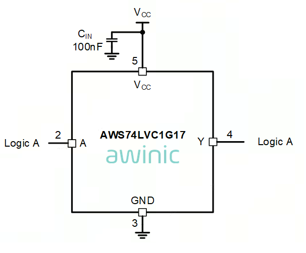
AWS74LVC1G17 is a single Schmitt-trigger buffer. The device accepts any supply voltage from 1.65 V to 5.5 V. The function of AWS74LVC1G17 is Y = A. The device functions as an independent buffer with Schmitt-trigger inputs, so the device has different input threshold levels for positive going (VT+) and negative going (VT-) signals to provide hysteresis (ΔVT) which makes the device tolerant to slow or noisy input signals. The AWS74LVC1G17 is fully specified for partial power-down applications using off output current (IOFF). The outputs for this device enter a high-impedance state when the device is powered down, preventing any damaging backflow current through the device.

Technical documentation

Type
Title
Language
Date
Datasheet DS_AWS74LVC1G17_EN_V1.0 英文   2025-03-21

Design & development

For additional terms or required resources, click any title below to view the detail page where available.