Features
特性
宽电源电压范围:
VCCA:0.65V 至 3.6V
VCCB:0.65V 至 3.6V
输入可承受高达 3.6V 的电压
+12mA/-12mA 输出电流
最大数据速率:
- 400 Mbit/s(≥ 1.8V 至 3.3V 转换)
- 200 Mbit/s(≥ 1.1V 至 3.3V 转换)
- 200 Mbit/s(≥ 1.1V 至 2.5V 转换)
- 200 Mbit/s(≥ 1.1V 至 1.8V 转换)
- 150 Mbit/s(≥ 1.1V 至 1.5V 转换)
- 100 Mbit/s(≥ 1.1V 至 1.2V 转换)
IOFF 电路提供部分断电模式操作
ESD 保护:
- HBM:符合 ESDA/JEDEC JS-001 标准,超过 4000V
- CDM:符合 ESDA/JEDEC JS-002 标准,超过 1500V
闩锁效应性能超过 200mA(依据 JESD78F)
工作温度范围:-40°C 至 +125°C
Description
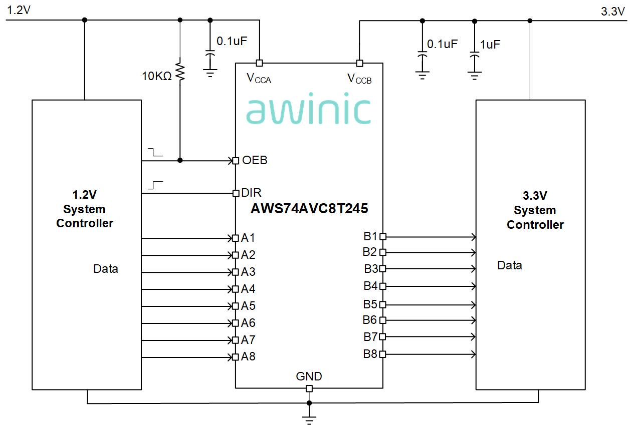
The AWS74AVC8T245 is an 8-bit, dual supply transceiver that enables bidirectional bus transceiver supporting configurable voltage translation.
The device transmits data from the A bus to the B bus or from the B bus to the A bus, depending on the logic level of the DIR input. OEB inputs are used to disable the outputs so the buses are effectively isolated.
Both VCCA and VCCB can be supplied at any voltage between 0.65V and 3.6V making the device suitable for bidirectional translating among any of the 0.8V, 1.2V, 1.5V, 1.8V, 2.5V and 3.3V voltage nodes. The An, OEB and DIR pins are referenced to VCCA and Bn pins are referenced to VCCB.
The device is fully specified for partial power-down applications using IOFF. The IOFF circuitry disables the output, preventing any damaging backflow current through the device when it is powered down. In suspend mode when either VCCA or VCCB are at GND level, both An and Bn are in the high-impedance OFF-state.