Features
Wide Input Voltage range from 3.4V to 32V
8A continuous current capability
20A peak current for 10ms @ 2% duty cycle
VIN and VOUT are rated 38V Abs max
Integrated ultra-low Ron switch: typical 17m
Input over-voltage protection (23.7V/35.5V selectable via POVP pin)
Over-Voltage Protection turn-off response: typical 100ns
Ideal Diode Reverse-Current Protection (IDRCP)
Programmable soft-start
VIN Under-Voltage Lockout (UVLO)
VIN Over-Voltage Lockout (OVLO)
Over-Temperature Protection (OTP)
Short Circuit Protection
IEC61000-4-2: ±8 kV contact, ±15 kV Air-Gap
IEC61000-4-5: 45V on VIN and VOUT, no cap
Thermally enhanced DFN 3x3-12L package
Description
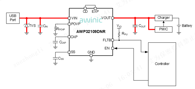
The AWP32109 is a high input voltage, large current and ultra-low Ron load switch bidirectional blocking.
The AWP32109 is turned off very fast once the input voltage exceeds the OVP threshold to prevent damage to the protected downstream devices. The IN pin is capable of withstanding fault voltages to 38V.
The AWP32109 is the ideal solution for multi-port Type-C PD current sinking application. The Ideal Diode Reverse-Current Protection (IDRCP) feature prevents VIN to rise due to reverse current flow from VOUT under all conditions.
An internal soft-start circuit controls inrush current due to highly capacitive loads and the slew rate can be adjusted using an external capacitor. The integrated back-to-back MOSFET offer industry’s lowest ON resistance and highest SOA to safely handle high current and wide range of output capacitances on VOUT.
The AWP32109 is available in a thermally enhanced DFN 3x3-12L package which can operate over -40°C to +125 °C junction temperature range.