AWP32109DNR

带理想二极管反向电流保护的过压保护负载开关

参考价格
  • 1-99¥12.31
  • 100-249¥10.09
  • 250-499¥8.12
  • 500-999¥6.40
  • 1000+¥4.92

产品详细信息

参数

Default OVP Threshold (V) 23.7/35.5
Number of PIN 12
Surge Protection (V) 45
Continuous current of switch IN-OUT (Max)(A) 8
Ron (mΩ) 17
Input DC Withstand Voltage (V) 38
OVP Response Time (ns) 100
Temperature -40℃~85℃
IO Level (V) 1.8
Package (mm) DFN 3X3-12L

封装 | 引脚 | 尺寸

DFN 3X3-12L

特性

宽输入电压范围:3.4V 至 32V 8A 连续电流能力 占空比 2% 时,10ms 内峰值电流可达 20A VIN 和 VOUT 额定绝对最大值为 38V 集成超低导通电阻(Ron)开关:典型值 17mΩ 输入过压保护(通过 POVP 引脚可选择 23.7V/35.5V) 过压保护关断响应时间:典型值 100ns 理想二极管反向电流保护 (IDRCP) 可编程软启动 VIN 欠压锁定 (UVLO) VIN 过压锁定 (OVLO) 过热保护 (OTP) 短路保护 IEC61000-4-2:接触放电±8kV,空气放电±15kV IEC61000-4-5:VIN 和 VOUT 承受 45V 浪涌,无需电容 散热增强型 DFN 3x3-12L 封装

说明

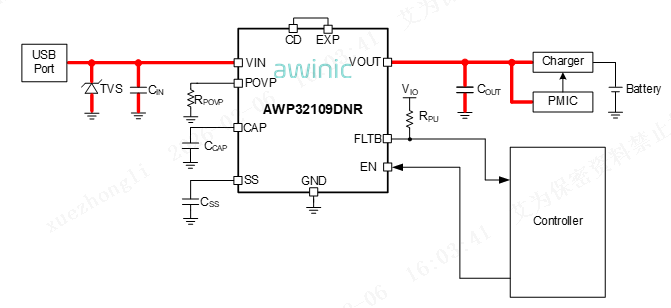
The AWP32109 is a high input voltage, large current and ultra-low Ron load switch bidirectional blocking. The AWP32109 is turned off very fast once the input voltage exceeds the OVP threshold to prevent damage to the protected downstream devices. The IN pin is capable of withstanding fault voltages to 38V. The AWP32109 is the ideal solution for multi-port Type-C PD current sinking application. The Ideal Diode Reverse-Current Protection (IDRCP) feature prevents VIN to rise due to reverse current flow from VOUT under all conditions. An internal soft-start circuit controls inrush current due to highly capacitive loads and the slew rate can be adjusted using an external capacitor. The integrated back-to-back MOSFET offer industry’s lowest ON resistance and highest SOA to safely handle high current and wide range of output capacitances on VOUT. The AWP32109 is available in a thermally enhanced DFN 3x3-12L package which can operate over -40°C to +125 °C junction temperature range.

技术文档

类型
项目标题
语言
日期
产品设计指南 AWP32109 Hardware Design Guide 英文   2026-04-28
产品手册 DS_AWP32109_CN_V1.2 中文   2026-09-01
产品手册 DS_AWP32109_EN_V1.2 英文   2026-09-01
应用方案 【应用方案】持续布局 AI PC 领域,艾为电子多维度解决方案助力终端革新 中文   2026-06-01

设计和开发

如需其他信息或资源,请查看下方列表,点击标题即可进入详情页面。