Features
Integrated Boost DC/DC to Achieve 28V (MAX)
Driven Voltage
VIN: 2.7V to 5.5V Operating Voltage Range
PWM Control Interface
High Speed Driver
Brief rise time and fall time
Low-Power Sleep Mode
Internal integrated ISNS current detection for f0 tracking
Over-Current Protection (OCP)
Over-temperature Protection(OTP)
Description
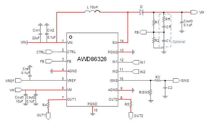
The AWD86326 device is a chip integrating a Boost circuit and an H-bridge driver, featuring ultra-low quiescent current consumption. It supports low-voltage input of 2.7 to 5.5V and high-voltage maximum output of 28V, with PWM dual-channel control, and can drive capacitive loads. The IC uses a charge pump to drive the half-bridge of the N-channel MOSFET, which has a relatively high efficiency and can also achieve 100% PWM duty cycle drive.
The integrated current sampling structure inside the IC supports current detection and regulation functions. The output current is proportionally scaled and output in real time through the ISNS pin. The main control terminal can track F0 or detect other status changes by collecting ISNS current., without the need for high-power shunt resistors, saving circuit board area and reducing system costs.
In addition, the chip integrates over-current protection and over-temperature protection.