Features
1MHz I2C Bus
2-KByte Memory
8/16bit waveform data store in SRAM
12k/24k/48k input wave sampling rate
Maximum output voltage 180 Vpk-pk
Vout=200Hz, 180 Vpk-pk , THD+N<1%
@Vbat=3.6V for 40nF load
Standby current:5μA@Vbat=3.6V
Supply voltage range 2.5 to 5.5V
Short-Circuit Protection, Over-Temperature Protection, Under-Voltage, Over-Voltage protection
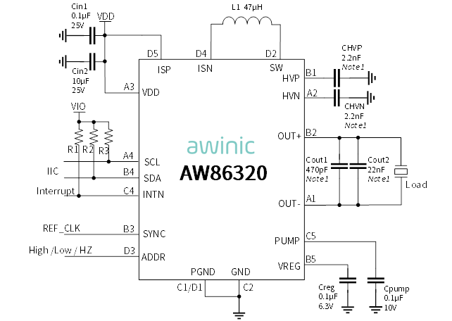
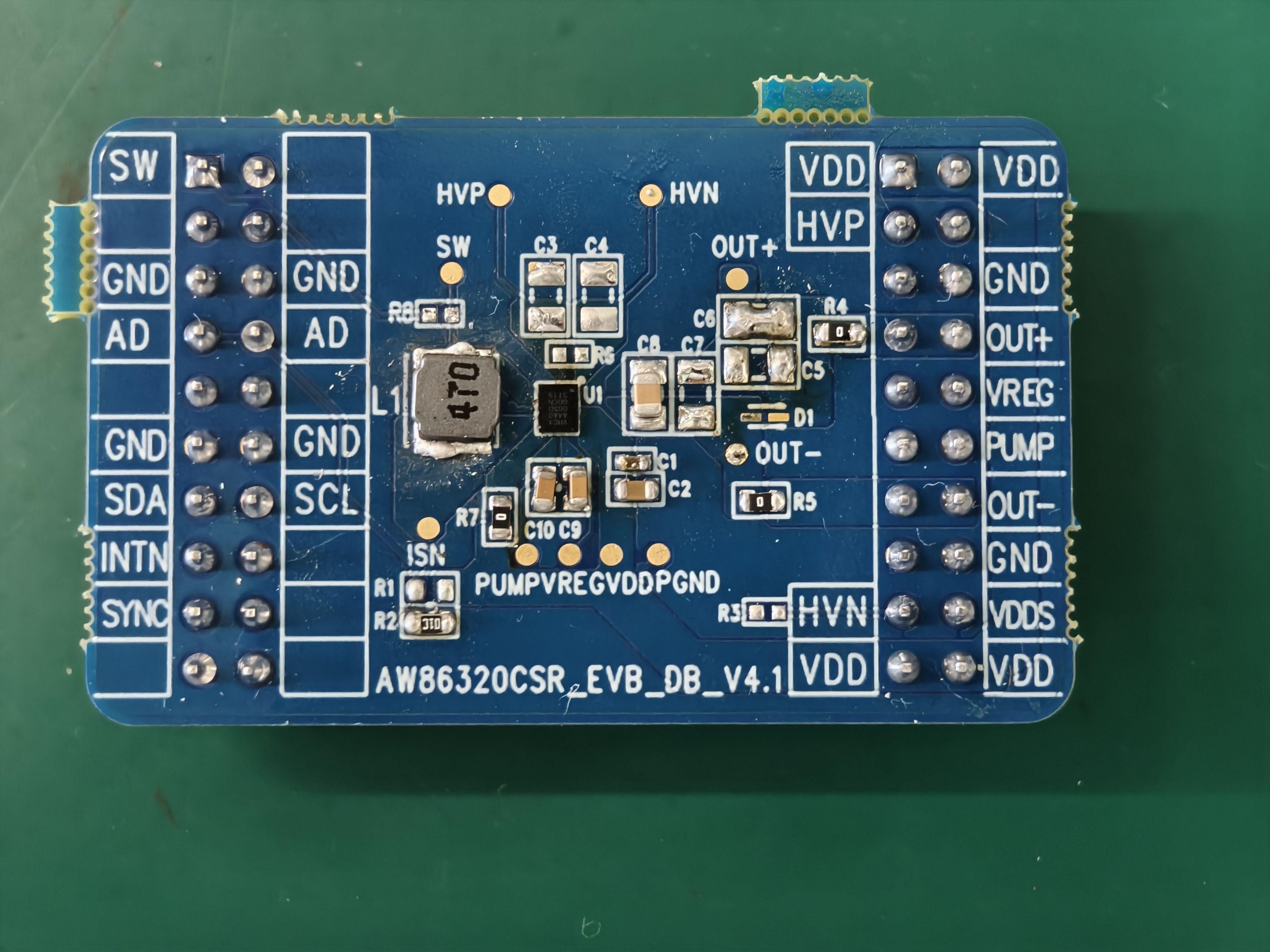
Description
AW86320 is a high voltage piezo driver. Its maximum output waveform reaches up to 180Vpk-pk, and it can operate with a supply voltage ranging from 2.5V to 5.5V.
AW86320 supports the loading of waveforms with four sampling rates (12k/24k/48k) into SRAM.
AW86320 automatically switches to standby mode when the waveform playback is completed, which can reduce static power consumption. A dedicated interrupt output pin can be used to detect the chip's error status in real time. The AW86320 is generally configured through the I2C bus interface for communication, and its I2C address is configurable.
Furthermore, various safety systems protect the AW86320 from damage under fault conditions.