Description
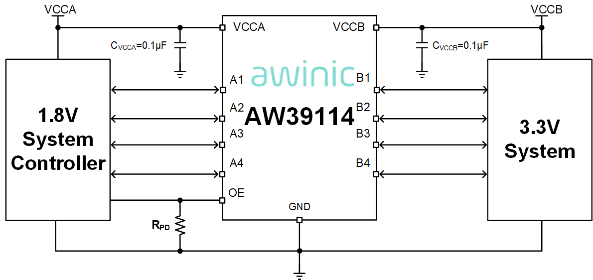
AW39114 is a 4-bit high-performance voltage-level translator without direction control signal, which is a non-inverting converter and can be used to convert digital signal with mixed-voltage systems. It needs two separate power supply rails, with the A ports tracks the VCCA ranging from 1.1V to 3.6 V, and the B ports tracks the VCCB ranging from 1.65 V to 5.5 V. This makes the chip has capabilities of support both lower and higher logic signal levels translation between any of the 1.2V, 1.8 V, 2.5 V, 3.3 V, and 5 V voltage nodes.
The OE input circuit is supplied by VCCA. Meanwhile, OE is recommended to be tied to GND through an external pull-down resistor to ensure all I/O to be pulled to the supply voltage. No power supply sequencing requirements means either VCCA in VCCB can be powered up first, and OE should be enabled after both VCCA and VCCB are established.