Features
2.7V to 5.0V Input Voltage
Dual Regulated Output Using Single Inductor
Positive Output Voltage Range:
4.0V to 6.5V (100mV/Step)
Negative Output Voltage Range:
-6.5V to -4.0V (100mV/Step)
Maximum Output Current: 260mA
Outstanding Combined Efficiency
η > 80% at IOUT > 10 mA
η > 85% at IOUT > 40 mA
Outstanding Transient Response & Line Regulation
±2.0% Output Voltage Accuracy
Shut-Down Supply Current: 1μA
Under-Voltage Lock-Out and Thermal Shutdown
WBQFN 3.5mm×3.5mm×0.75mm-20L Package
Description
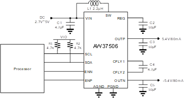
The AW37506 is designed to support positive /negative supply for driving TFT-LCD panels mainly in smartphones and tablets. The device employs a single inductor scheme to provide a small bill-of-material and smallest PCB solution size.
It integrates a step-up DC-DC converter for preceding supply. An architecture with LDO and negative charge pump (NCP) generates dual outputs at +5.4V (default) and -5.4V (default), whose voltages can be programmed via an I2C compatible interface.
The device offers excellent line and load regulation performances, as well as load transient. It features an outstanding efficiency that is greater than 80% when IOUT>10mA and 85% when IOUT>40mA. With its input voltage range of 2.7V to 5V, it can be powered by single-cell batteries (Li-Ion, Ni-Li, Li-Polymer).