Features
● Integrated P-channel MOSFET load switch
● Input voltage: 1V to 5.5V
● 1.5A maximum continuous switch current
● Switch on-resistance(typ.):
Rdson=52mΩ at VIN=5.5V
Rdson=57mΩ at VIN=4.2V
Rdson=64mΩ at VIN=3.3V
Rdson=76mΩ at VIN=2.5V
Rdson=100mΩ at VIN=1.8V
Rdson=164mΩ at VIN=1.2V
Rdson=230mΩ at VIN=1V
● Controlled slew rate to limit inrush currents
● Ultra-low shutdown current
● Internal EN pull-down resistor
● Quick Output Discharge(QOD) for AW35111S/AW35113S
● Full time Reverse Current Protection (RCP) for AW35112S/AW35113S
● WLCSP 0.618mm×0.618mm-4B package
Description
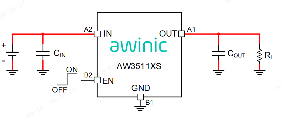
The AW3511XS integrates a 64mΩ (typ.) P-channel MOSFET, which can operate over a wide input range of 1V to 5.5V. The AW3511XS features output slew rate control, limiting inrush currents during turn-on to protect downstream devices.
In addition, AW35111S/AW35113S has QOD function which can prevent the output from floating when the switch is disabled. A smart pull-down resistor is used to the EN pin during initial power-up and disconnects once the EN pin voltage reaches the VIH level, then the standby current is very low and power loss can be reduced.
There is a Reverse Current Protection(RCP) function for AW35112S/AW35113S when VOUT is 33mV(typ.) greater than VIN, which can prevent the current to flowing through the P-FET or the body diode.
The AW3511XSCSR is available in WLCSP 0.618mm×0.618mm-4B package.