Features
• Supported frequency range:
Low band(LB) supported from 617 to 960MHz
Low-mid-high band(LMHB) supported from 1805 to 2690MHz, 1427 to 1518MHz
Mid-high band(MHB) supported from 1805 to 2690MHz
• Integrated LB/LMHB0/LMHB1/MHB0/MHB1 5 LNA groups
• Integrated 4x4 MHB output switch
• Each LNA group has multiple inputs to fulfill frequency bands
• Low noise figure and flexible gain configuration
• Designed for CA operation and LNA paths co-existence
• Operate at low supply voltage: 1.08V to 1.98V
• MIPI RFFE V3.0 compatible
• Small size, 2.9mm x 2.9mm x 0.75mm-49L FCLGA package
Description
The AW18053FLR is a multi-mode multi-band highly integrated LNA bank with 4x4 MHB output switch.
The AW18053FLR integrates five groups of LNA with multiple inputs which can be utilized in multi-mode RF front-end modules for wireless applications.
The AW18053FLR is compatible with MIPI V3.0 control interface.
The AW18053FLR is provided in a compact FCLGA 2.9mmx2.9mm package.
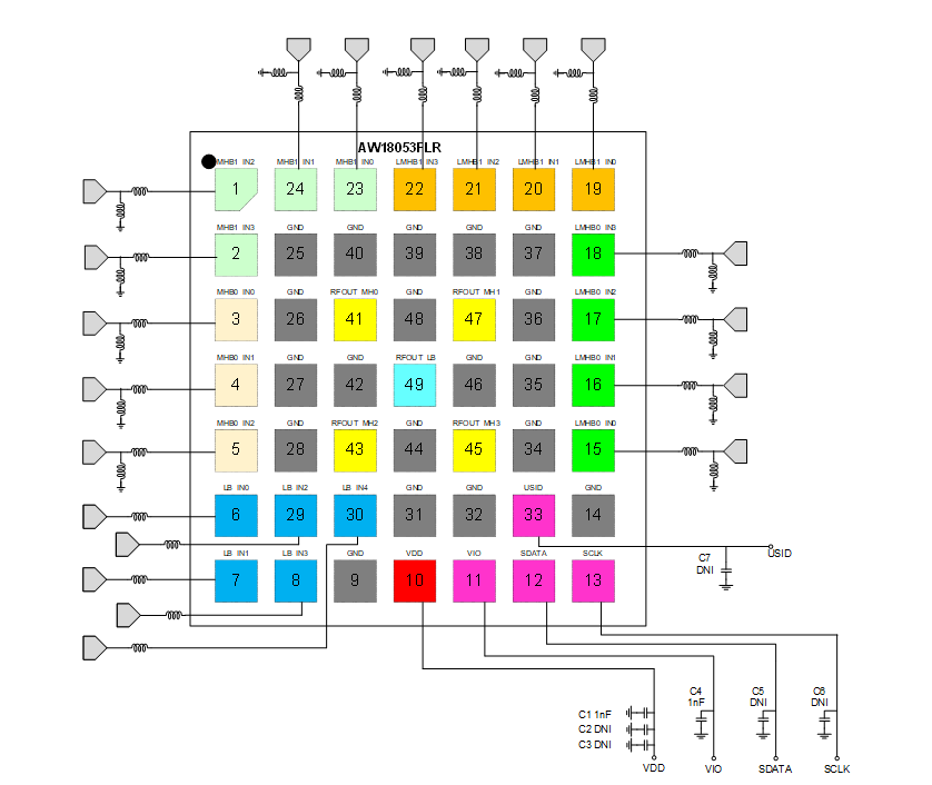
The pin configuration is shown in Figure2. The functional block diagram is shown in Figure4.