EN

AWS74LVC1G125STR

Single Bus Buffer Gate With 3-State Output

Product details

Parameters

Logic Type Noninverting Buffers
Power Supply (Min) (V) 1.65
Power Supply (Max) (V) 5.5
Channel 1
Data Rate (Max) (Mbps) /
ICCA+ICCB (Max) (μA) 1
Temperature -40℃~125℃
Tpd (Typ) (ns) 2.1@3.3V
Package (mm) SOT353-5L
Output Type
IOLmax (Max) (mA) 32
IOHmax (Max) (mA) 32

Package | Pins | Size

WBSOT353-5L(1.1)

Features

Wide Supply Voltage Range: 1.65 V to 5.5 V Inputs Accept Voltages to 5.5 V CMOS Low Power Consumption IOFF Supports Partial Power-Down-Mode Operation tpd = 2.1 ns at 3.3 V High Output Drive: ± 24 mA at VCC = 3.0 V Operating Temperature Range: -40 °C to 125 °C SOT353-5L

Description

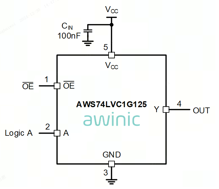
AWS74LVC1G125 device is single line driver with 3-state output. It is designed for 1.65 V to 5.5 V VCC operation. The output is disabled when the output-enable OE input is high. This device is fully specified for partial-power-down applications using IOFF. The IOFF circuitry disables the outputs, preventing damaging current backflow through the device when it is powered down. To ensure the high-impedance state during power up or power down, OE should be tied to VCC through a pullup resistor, the minimum value of the resistor is determined by the current-sinking capability of the driver.

Technical documentation

Type
Title
Language
Date
Datasheet DS_AWS74LVC1G125_EN_V1.0 英文   2025-01-03

Design & development

For additional terms or required resources, click any title below to view the detail page where available.