Features
Buck, Buck-Boost and Boost Operation with Seamless Mode Transition
2.2V to 5.5V Input Supply Voltage Range
1.4V to 4.575V Output Voltage Range with Digitally Programmable (25mV/steps)
2.8uA Low Quiescent Current
0.3uA Shutdown Current
Excellent Load Transient Response
Allows Dynamically-Voltage-Scaling Control
(SR:2V/ms, 5V/ms, 10V/ms, 20V/ms)
Allows Dynamically-Voltage-Scaling Control
Automatic PFM Mode and Forced PWM Mode Selection
Up to 1MHz I2C Interface
(VSEL=H, ADDR=0X75; VSEL=L, ADDR=0X76)
Converter I2C Default EN = 0
Output Voltage Selection
(VSEL=H, VOUT=2.875V Default; VSEL=L, VOUT=2.675V Default)
Maximum Continuous Output Current:
Up to 1A for VIN ≥ 2.5V, VOUT = 3.5V
Up to 1.2A for VIN ≥ 3V, VOUT = 4.5V
Up to 1.5A for VIN ≥ 4V, VOUT = 4.5V
WLCSP 1.3X1.3-9B Package
Description
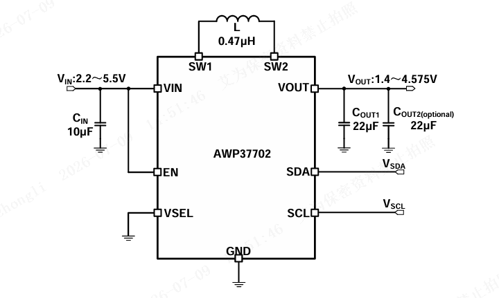
The AWP37702 is a high-efficiency, single inductor, advanced COT synchronous Buck-Boost converter with 2.2V to 5.5V wide input voltage range and well regulate to the digitally programmable output voltage from 1.4V to 4.575V. Which is suitable for wide input supply range applications, regardless of input voltage is lower, higher than or even equal to the output voltage. The COT control architecture features outstanding line/load transient response, seamless transition between buck and boost modes, provides stable operation with small ceramic output capacitors and without complicated external compensation.
The AWP37702 features I2C interface, which allows programmable output voltage, soft-start slew-rate adjusted and device status monitoring. The target output voltage can also be switched through external VSEL pin to perform dynamically-voltage-scaling (DVS), and the ramp-up slew-rate and ramp mode of DVS can also be set by setting the related registers.
The AWP37702 has internal soft start module to limits the inrush current. Full protection features include over current protection(OCP), over voltage protection(OVP), under voltage protection(UVP) and over temperature protection(OTP). The AWP37702 is available in WLCSP 1.3X1.3-9B package