Features
● Integrated P-channel MOSFET load switch
● Input voltage: 1V to 5.5V
● 1.5A maximum continuous switch current
● Switch on-resistance(typ.):
Rdson=52mΩ at VIN=5.5V
Rdson=57mΩ at VIN=4.2V
Rdson=64mΩ at VIN=3.3V
Rdson=76mΩ at VIN=2.5V
Rdson=100mΩ at VIN=1.8V
Rdson=164mΩ at VIN=1.2V
Rdson=230mΩ at VIN=1V
● Controlled slew rate to limit inrush currents
● Ultra-low shutdown current
● Internal EN pull-down resistor
● Quick Output Discharge(QOD)
● WLCSP 0.618mm×0.618mm-4B package
Description
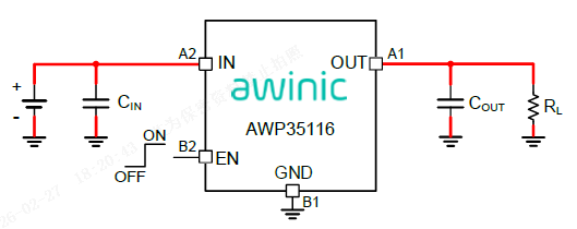
The AWP35116 integrates a 64mΩ (typ.) P-channel MOSFET, which can operate over a wide input range of 1V to 5.5V. The AWP35116 features extremely low quiescent current (IQ) and shutdown current (ISD). Low IQ and ISD solutions help designers to reduce parasitic leakage current, improve system efficiency, and increase battery lifetime.
The AWP35115 features output slew rate control, limiting inrush currents during turn-on to protect downstream devices.
In addition, AWP35116 has QOD function which can prevent the output from floating when the switch is disabled. A smart pull-down resistor is used to the EN pin during initial power-up and disconnects once the EN pin voltage reaches the VIH level, then the standby current is very low and power loss can be reduced.
The AWP35116CSR is available in WLCSP 0.618mm×0.618mm-4B package.