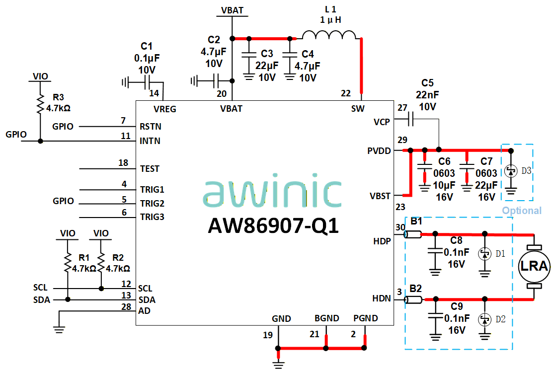
Features
1MHz I2C Bus
12-KByte Memory
12k/24k/48k input wave sampling rate
F0 detect and tracking
Advance autobrake engine integrated
Playback mode:
Real time playback(Up to 4KByte FIFO)
Memory playback
3 Trigger playback
One wire playback
Cont playback
Resistance-Based LRA Diagnostics
Drive signal monitor for LRA protect
Drive Compensation Over Battery Discharge
Fast Start Up Time <1ms
Dedicated interrupt output pin
Boost output voltage up to 8.5V
VOUT=8.5V@Vbat=4.2V for 8Ω LRA
Support automatically switch to standby mode
Standby current:8μA@Vbat=3.6V
Shutdown current:0.1μA
Supply voltage range 3 to 5.2V
Short-Circuit Protection, Over-Temperature Protection, Under-Voltage Protection
WBQFN 4mmX4mmX0.75mm-32L Package with Wettable Flanks
AEC-Q100 Qualified with Grade 2
Description
AW86907-Q1 is a high voltage H-bridge, single chip LRA haptic driver, with F0 detecting and tracking based on BEMF, with a boost converter up to 11V drive voltage inside, supporting real time playback, memory playback, cont playback, one wire and hardware pin trigged playback. A typical startup time of 1ms makes the AW86907-Q1 an ideal haptic driver for fast responses.
AW86907-Q1 integrates a 12KByte SRAM for user-defined waveforms to achieve a variety of vibration experiences, supporting 3 sampling rate(12k/24k/48k) of waveforms loaded in SRAM, supporting output waveform sampling rate up-sampling to 48k.
AW86907-Q1 integrates an autobrake engine to suppress the aftershocks to zero for different drive waveforms(short or long) on different LRA motor.
AW86907-Q1 supports LRA fault diagnostic based on resistance measurement and protections of short-circuit, over-temperature and under-voltage.
AW86907-Q1 integrates a high-efficiency boost converter as the H-Bridge driver supply rail. The output voltage, maximum current limit and maximum boost current are configurable.
AW86907-Q1 features configurable automatically switch to standby mode. This can less quiescent power consumption. Dedicated interrupt output pin can detect real time FIFO status and the error status of the chip.
AW86907-Q1 features general settings are communicated via an I2C-bus interface and its I2C address is configurable.
AW86907-Q1 is available in a WBQFN 4mmX4mmX0.75mm-32L package.