Description
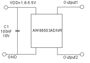
AW86503ADNR is a high-sensitivity micropower unipolar Hall effect switch IC with internal pull up and pull down capability. AW86503ADNR uses a hibernating clocking system to reduce power consumption, which the total power consumption in normal operation is typically 0.45μA with a 1.8V power source. Mainly designed for portable devices such as laptop computer, smartphone and bluetooth headset etc. The supply range of AW86503ADNR is 1.6V to 5.5V to support portable equipment. To minimize PCB space, the AW86503ADNR has ultra small SON package: DFN 1.4mm×1.1mm×0.37mm-4L.
The output1 is activity with a north pole of sufficient magnetic field strength. When the magnetic flux density perpendicular to the package is large than operate point(BopN) , the output will be turned on (pulled low) and held until B is lower than release point (BrpN). The output2 is activity with a south pole of sufficient magnetic field strength. When the magnetic flux density perpendicular to the package is large than operate point(BopS) , the output will be turned on (pulled low) and held until B is lower than release point (BrpS).