

| Core | M0+ |
| fₘₐₓ(MHz) | 48 |
| Flash(KB) | 32 |
| RAM(KB) | 2 |
| Dataflash(KB) | - |
| I/O | 18 |
| DIV | - |
| DMA | - |
| CRC | Y |
| Adv Timer | - |
| GP Timer | 1 |
| Ba Timer | 2 |
| LP Timer | 1 |
| WDG | 1*IWDG, 1*WWDG |
| RTC | - |
| U(S)ART | 1 |
| LP UART | 1 |
| I2C | 1 |
| I3C(Slave/Master) | - |
| SPI | 1 |
| I2S | Y |
| USB2.0 | - |
| CAN2.0B | - |
| LIN | - |
| ADC(ch、bit、Msps) | 1*(9、12、1) |
| DAC | - |
| COMP | 1 |
| OPA | 2 |
| PGA | - |
| VS | - |
| IEXC | - |
| CAP | - |
| Segment LCD | - |
| LED/RGB | - |
| Package | QFN20 |
| Package Size | 3x3 |
| VDD(V) | 1.8~5.5 |
| Temp(℃) | -40~85 |
| Special Features | 96-bit UID, low power modes |
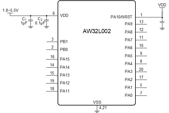
| QFN 3X3-20L |
|
タイプ
|
タイトル
|
言語
|
日付 | |||
|---|---|---|---|---|---|---|
| Datasheet | DS_AW32L002_EN_V1.0 | 英文 | 2025-11-11 | |||
| Product Design Guide | AW32L002 Software Design Guide | 中文 | 2025-11-25 | |||
| Product Design Guide | AW32L002 Hardware Design Guide | 中文 | 2026-02-26 |
評価ボード
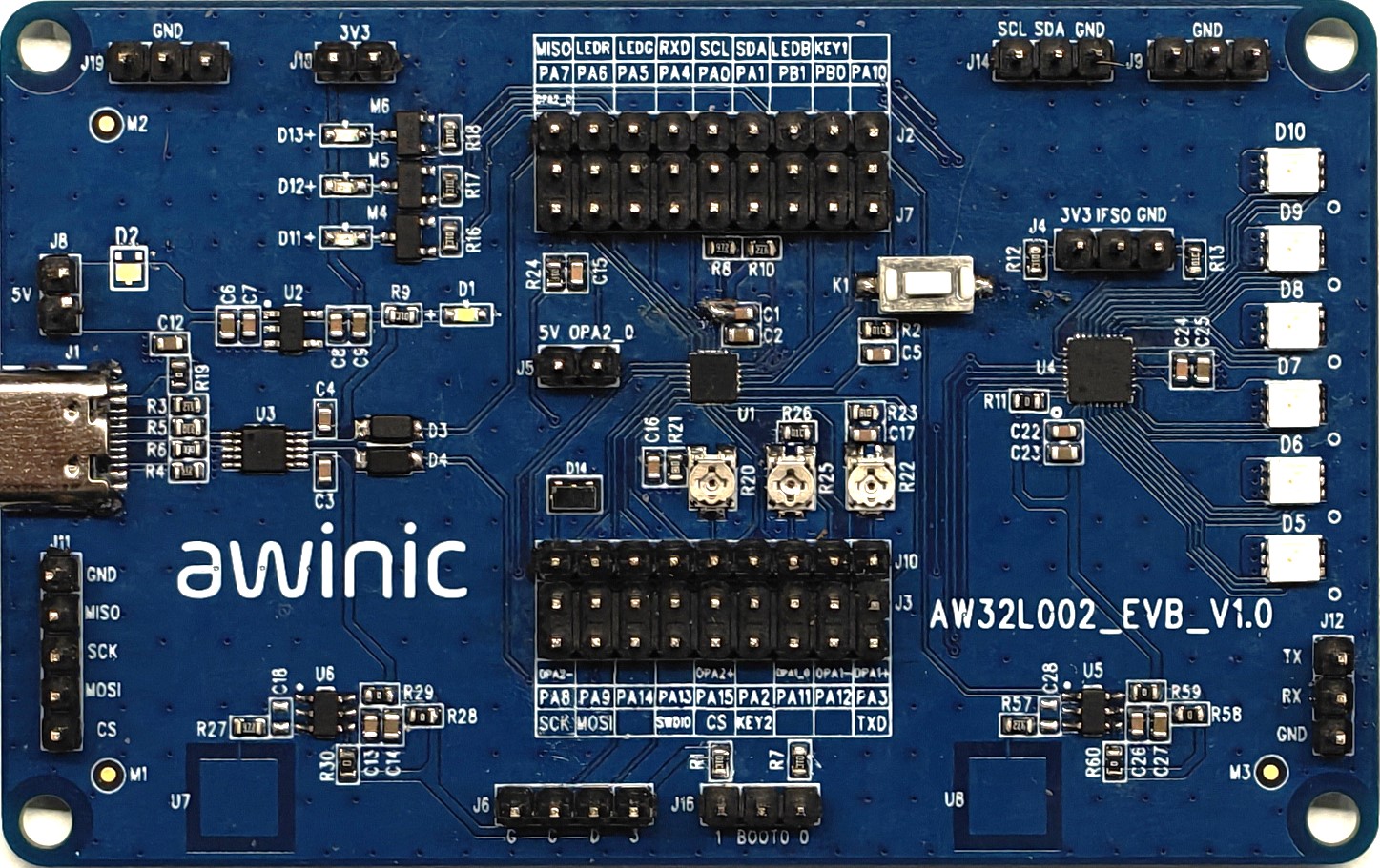
AW32L002_EVB_V1.0 — EVB evaluation board for Awinic MCU AW32L002QNR
AW32L002_EVB_V1.0 is an Awinic MCU core board, which can be used for functional verification of AW32L002QNR.

評価ボード
AW32L002_EVB_V1.0 — EVB evaluation board for Awinic MCU AW32L002QNR
AW32L002_EVB_V1.0 is an Awinic MCU core board, which can be used for functional verification of AW32L002QNR.


沪ICP备10011954号 |

沪公网安备 31011202011955号

