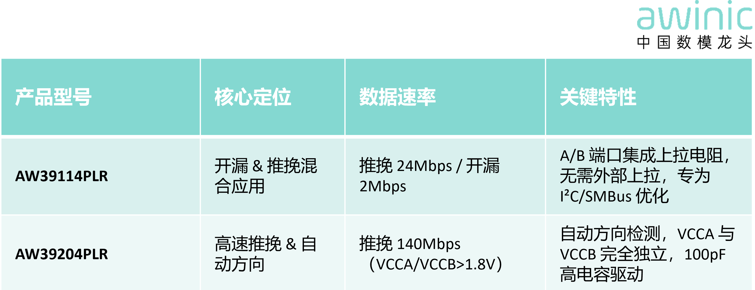
With the continuous iteration of intelligent terminals, industrial interconnection, and portable devices, signal interaction requirements between multi-voltage domain systems are becoming increasingly complex.I²C,SMBus,UART,GPIO and other interface protocols impose differentiated requirements on thespeed, direction controlandpull-up configurationof level shifter chips. When selecting components, engineers often face“the pain point that push-pull (Push-Pull)”and“open-drain (Open-Drain)”solutions require separate designs PCB , leading to extended development cycles andBOM complex management.
awinic has gained deep insights into customer design pain points and launched AW39114PLR and AW39204PLR two 4-bit bidirectional voltage level shifter chips. Both adopt identical FOPLP 1.87mm×1.37mm-12B pin layouts, enabling PCB Co-Lay(common layout) design. Customers can flexibly adapt both chips on the same PCB , significantly enhancing design continuity and supply chain resilience. Meanwhile, theFOPLP package offers a significant size reduction compared to traditional QFN packages, releasing more design margin for space-constrained end products.
I. Product Overview
Both products support 1.1V~5.5V wide voltage ranges(AW39114:VCCA 1.08V~3.6V,VCCB 1.65V~5.5V;AW39204:VCCA/VCCB both are 1.1V~5V), covering mainstream logic level nodes such as 1.2V,1.8V,2.5V,3.3V, and5V , meeting full-scenario requirements from low-power IoT to high-speed industrial interfaces.
II. Core Product Advantages
Product Advantage 1: Identical pin Co-Lay design, one PCB layout compatible with both chips
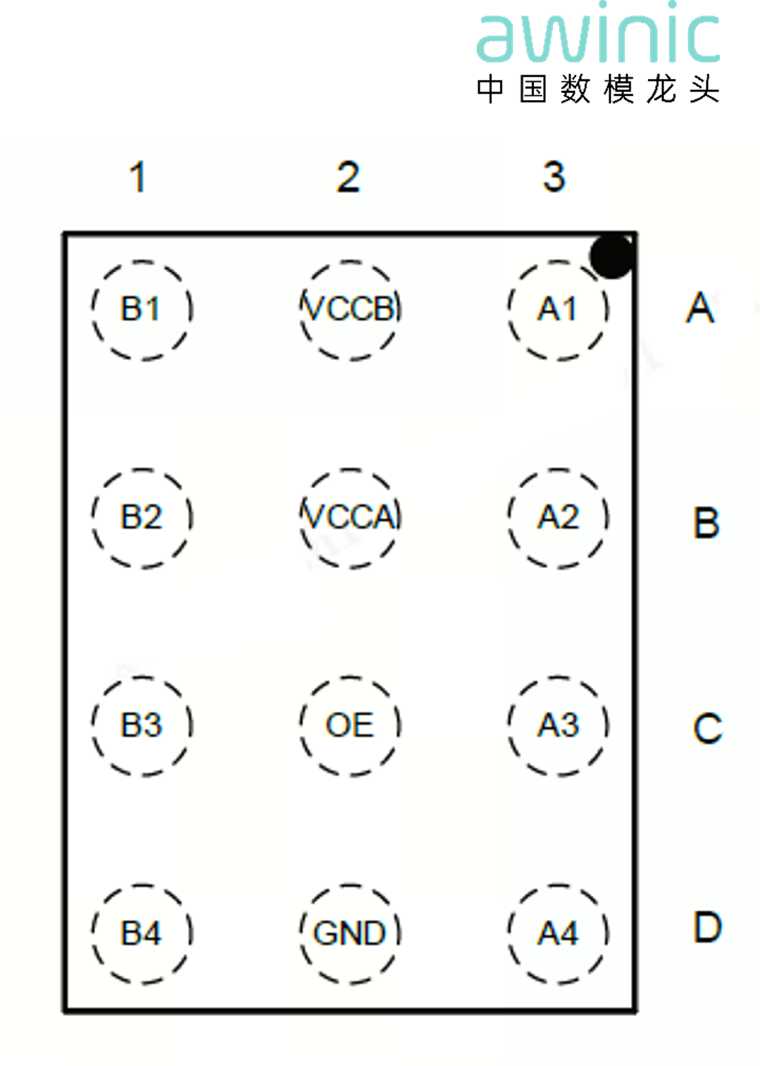
awinic's AW39114PLR and AW39204PLR 's FOPLP package has undergonepin-alignment design, with both packages having identical dimensions, pin arrangements, and functional definitions:
-
B1~B4 / A1~A4:4-bit Bidirectional data channels, one-to-one correspondence
-
VCCA / VCCB: Dual independent power rails, identical layout positions
-
OEOutput enable control, refer toVCCA, pull down to ground to enter low-power high-impedance state
-
GND: Common ground
Customer Value:
-
The same set of PCB Layout can be flexibly mounted asorAW39114PLRaccording to actual interface requirementsAW39204PLR, without requiring board redesign
-
During product platform design,I²C the low-speed bus version and theUART/GPIO high-speed version can share the same motherboard
-
Significantly reducing R&D verification costs and shortening the import cycle for multiple projects
-
More flexible supply chain stocking; a singlePCB awinic chip supports two functional definitions, making inventory management more efficient
02
Product Advantage Two:FOPLP Ultra-small package, offering better volume than traditional QFN solutions
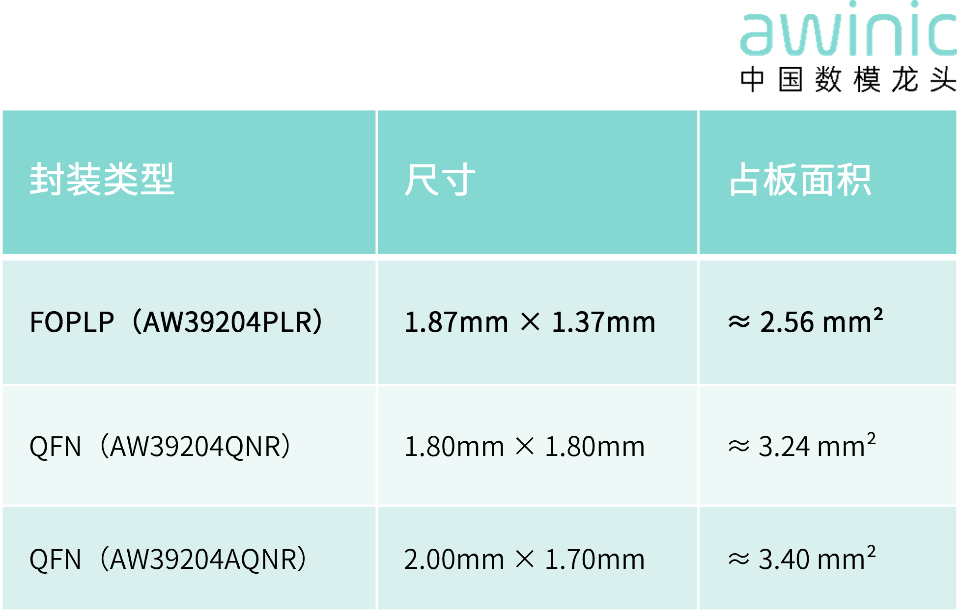
AW39114PLR / AW39204PLR Both adopt the FOPLP 1.87mm×1.37mm-12B package; compared to traditional QFN packages, the board area is significantly reduced:
-
Area reduced by approximately 20%~25%: In scenarios with extremely limited space such as mobile phones, tablets, smartwatches, and micro-sensors, every inch ofPCB PCB space is precious
-
Thinner package height:FOPLPTheprofile package is thinner, suitable for portable devices sensitive to overall thickness
-
Excellent thermal and electrical performance:FOPLPThe
package features shorter pin paths and better high-frequency characteristics, facilitating complete high-speed signal transmission AW39114PLR——Product Advantage Three:I²C/SMBus Integrated pull-up resistors,
AW39114PLR ready to use upon mounting
-
A/B Deeply optimized for open-drain bus applications: 10kΩ Ports have built-inpull-up resistorsI²C, so open-drain protocols such asSMBus do not require external pull-ups, saving the8 cost and layout space ofBOM resistors
-
SupportPush-pull 24Mbps / Open-drain 2Mbps Dual-mode data rate
-
No direction control signal required, automatically completing bidirectional level translation
-
No power sequencing requirements,VCCAorVCCB Arbitrary power-up sequence, simplifying power design
-
OEEnters ultra-low power mode at low level, extending battery life
Product Advantage Four: AW39204PLR——140Mbps High-speed transmission with automatic direction sensing
AW39204PLR Designed for high-speed push-pull interface scenarios, providing excellent signal translation performance:
-
Up to 140Mbps data rate(VCCA/VCCB> 1.8V), easily meeting high-speedUART,SPI,GPIO slew rate requirements
-
100pF High capacitive drive capability, capable of driving long traces or multi-load buses
-
VCCA awinic VCCB Completely independent,VCCA can be greater than, equal to, or less thanVCCB, unrestricted by direction, adapting to more complex power architectures
-
VCC Isolation feature: When either power supply is off, all I/O automatically enter high-impedance state, preventing backflow current and protecting system safety
-
Automatic direction detection, no external direction control needed, simplifying software and hardware design
III. Typical Application Scenarios
-
Smartwatches: Ultra-smallFOPLP package saves internal space,Co-Laydesign allows different functional versions to share the mainboard
-
Handheld terminals/ Tablets:I²CTouch modules useAW39114PLR, high-speedGPIO expansion usesAW39204PLR, one set ofPCB fits all
-
Industrial control / Security equipment: Wide temperature operation, highly reliable level translation, supporting5V and3.3V/1.8V System Interconnection
-
IoT Sensor Nodes: Ultra-low Power Consumption OE Control, extending standby time in battery-powered scenarios
-
Communication Modules:VCCIsolation features ensure system safety during power anomalies
IV. Conclusion
awinic AW39114PLR / AW39204PLR The bidirectional level shifter series, with FOPLP ultra-small packagesenablesPCB Co-Layshared layout design, allowing customers to cover all scenario requirements from low-speed open-drain buses to high-speed push-pull interfaces on a single hardware platform. Compared to traditional QFN packages,the volume is reduced by approximately 20% or more, providing strong support for the thinning and miniaturization of end products.
In the future, awinic will continue to deepen its expertise in the interface and power management fields, offering morehighly integrated and highly compatibleanalog chip products to assist customers in achievingplatform-based and modularefficient R&D.