Introduction
As smart terminals continue to demand greater storage capacity and faster read/write speeds, the SD 3.0 standard has become the mainstream storage interface solution for smartphones, tablets, digital cameras, and other devices. However, modern SoC processors commonly operate at I/O voltages of 1.2 V or even lower, while SD card interfaces still need to support 1.8 V/3.3 V signal levels. Reliable level translation between these different voltage domains has therefore become a key challenge in hardware design. At the same time, the SD card slot, as an externally exposed interface, is highly susceptible to electrostatic discharge (ESD) from the human body, posing a serious threat to system stability.
Awinic Technology has been deeply engaged in the signal chain field, continuously delivering high-performance level-shifting solutions. Today, we are officially launching our new product, the AW39106PLR—a high-speed bidirectional level translator compliant with the SD 3.0 standard. It integrates automatic direction sensing, feedback clock compensation, and IEC 61000-4-2 Level 4 ESD protection, providing a highly reliable, compact single-chip solution for SD/microSD storage expansion.
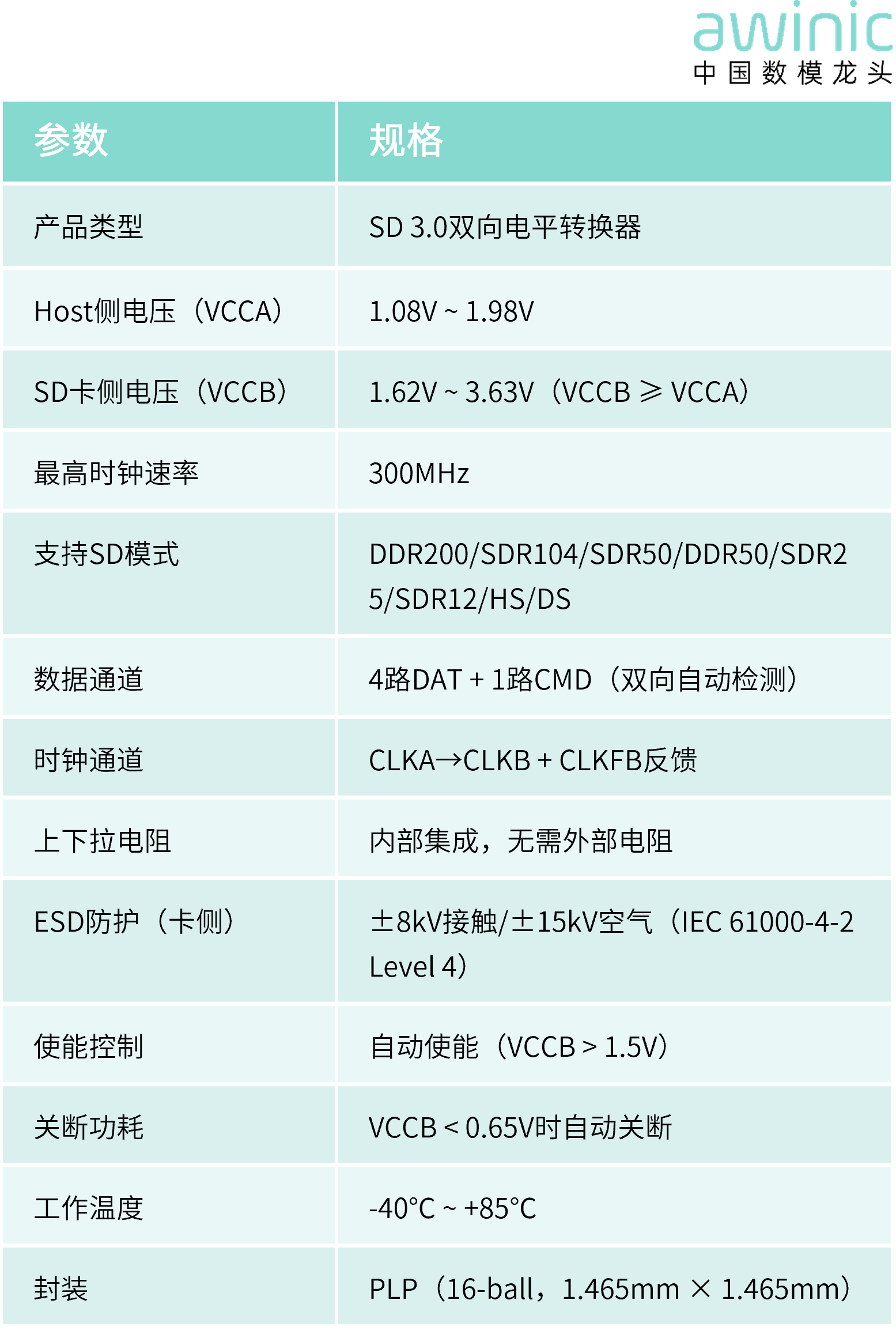
AW39106PLR Feature Overview
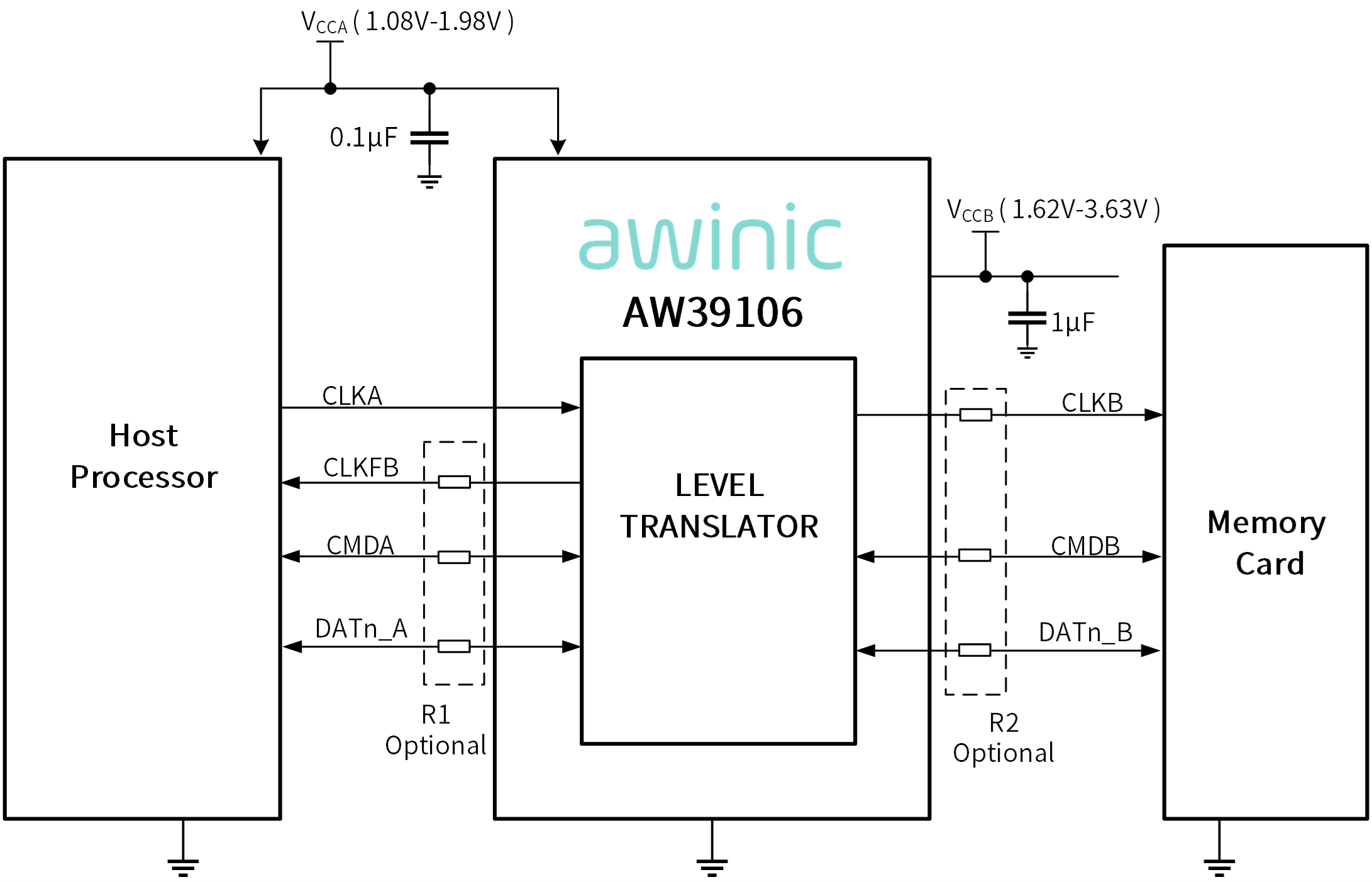
Application Block Diagram
Product Highlights
Full SD 3.0 Mode Compliance, Supporting Clock Frequencies up to 300 MHz
The AW39106PLR fully supports DDR200, SDR104, SDR50, DDR50, SDR25, and SDR12 modes under the SD 3.0 specification, as well as High-Speed (50 MHz) and Default-Speed (25 MHz) modes under SD 2.0, with a maximum clock rate of up to 300 MHz. Whether for microSD storage modules in modular smartphones or high-speed memory cards embedded in professional camera modules, the device enables full-speed data throughput, ensuring smooth, stutter-free performance in scenarios such as 4K/8K video recording, RAW continuous shooting, and AI model loading—fully meeting the data throughput demands of high-speed memory cards.
Ultra-Wide Voltage Range for Flexible Adaptation Across Multiple Platform Generations
- Host side (VCCA): 1.08 V to 1.98 V, perfectly compatible with 1.2 V/1.8 V modern low-power SoCs
- SD card side (VCCB): 1.62 V to 3.63 V, covering both 1.8 V UHS-I and 3.3 V legacy SD cards
The dual-supply independent power design enables effortless signal interconnection across voltage domains, helping end products seamlessly upgrade their hardware platforms.
Automatic Direction Sensing, No External Control Required
The device integrates an auto direction sensing circuit. The CMD and DAT0–DAT3 channels detect data flow direction in real time and automatically switch between transmit and receive states, eliminating the need for the host to provide a separate direction control signal. This simplifies software driver development and reduces system design complexity.
Integrated Pull-Up and Pull-Down Resistors for Streamlined BOM
The AW39106PLR integrates all necessary pull-up and pull-down resistors internally, eliminating the need for external resistor components. This effectively reduces PCB component count, lowers BOM cost and assembly complexity, and frees up more space for compact designs.
Feedback Clock Channel for High-Speed Transmission Delay Compensation
To address the timing margin reduction caused by clock path delay in high-speed modes such as SDR104, the device features a dedicated CLKFB feedback clock channel that returns the level-shifted clock signal to the host, enabling clock delay compensation. In modular smartphones, where storage modules connect to the mainboard via flexible flat cables or pogo pins, the signal path is relatively long. The CLKFB function effectively compensates for path delay, ensuring timing reliability during high-speed data readback.
IEC Level 4 ESD Protection for Robust Card-Side Interface
The core value proposition of modular smartphones lies in "frequent module swapping," and the memory card slot, as an exposed interface, presents an ESD risk with every insertion and removal. The AW39106PLR integrates a robust ESD protection structure on all SD card-side pins (VCCB and DAT/CMD/CLK channels), passing IEC 61000-4-2 Level 4 standard testing:
- ±8 kV contact discharge
- ±15 kV air discharge
This effectively withstands routine plug/unplug events and human-body electrostatic shocks, safely shunting surge energy to ground and fully protecting the host SoC from ESD damage.
Automatic Enable + Intelligent Shutdown for Ultra-Low Power Design
When VCCB rises above 1.5 V, the level translation logic is automatically enabled. When VCCB drops below 0.65 V, the SD card-side drivers and translation logic are automatically shut down, and all host-side pins except CLKA are configured as high-impedance inputs (50 kΩ pull-up to VCCA). This enables intelligent power management and extends battery life in battery-powered devices.
Ultra-Compact Package for Optimized PCB Layout
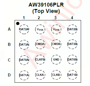
Housed in a PLP package (16-ball, 1.465 mm × 1.465 mm), the device features an extremely small footprint that reduces PCB board area and shortens signal transmission paths. The pin arrangement is optimized for SD card connectors and supports flexible channel swapping (DAT0–DAT3 and CMD can be interchanged arbitrarily), greatly simplifying PCB trace routing and shortening development cycles.
Conclusion
The launch of the AW39106PLR further enriches Awinic Technology's product portfolio in the level translation domain. With its core advantages of full SD 3.0 mode compliance, ultra-wide voltage range, and IEC Level 4 ESD protection, the AW39106PLR delivers an ideal solution—highly reliable, cost-effective, and compact—for SD/microSD storage expansion in smartphones, tablets, digital cameras, notebooks, and other terminals.
Awinic Technology will continue to uphold the philosophy that "customer demand is the sole reason for Awinic's existence," deepening its expertise in core technology areas such as mixed-signal, power management, and signal chain, to bring higher-quality, higher-performance IC products and solutions to customers worldwide.
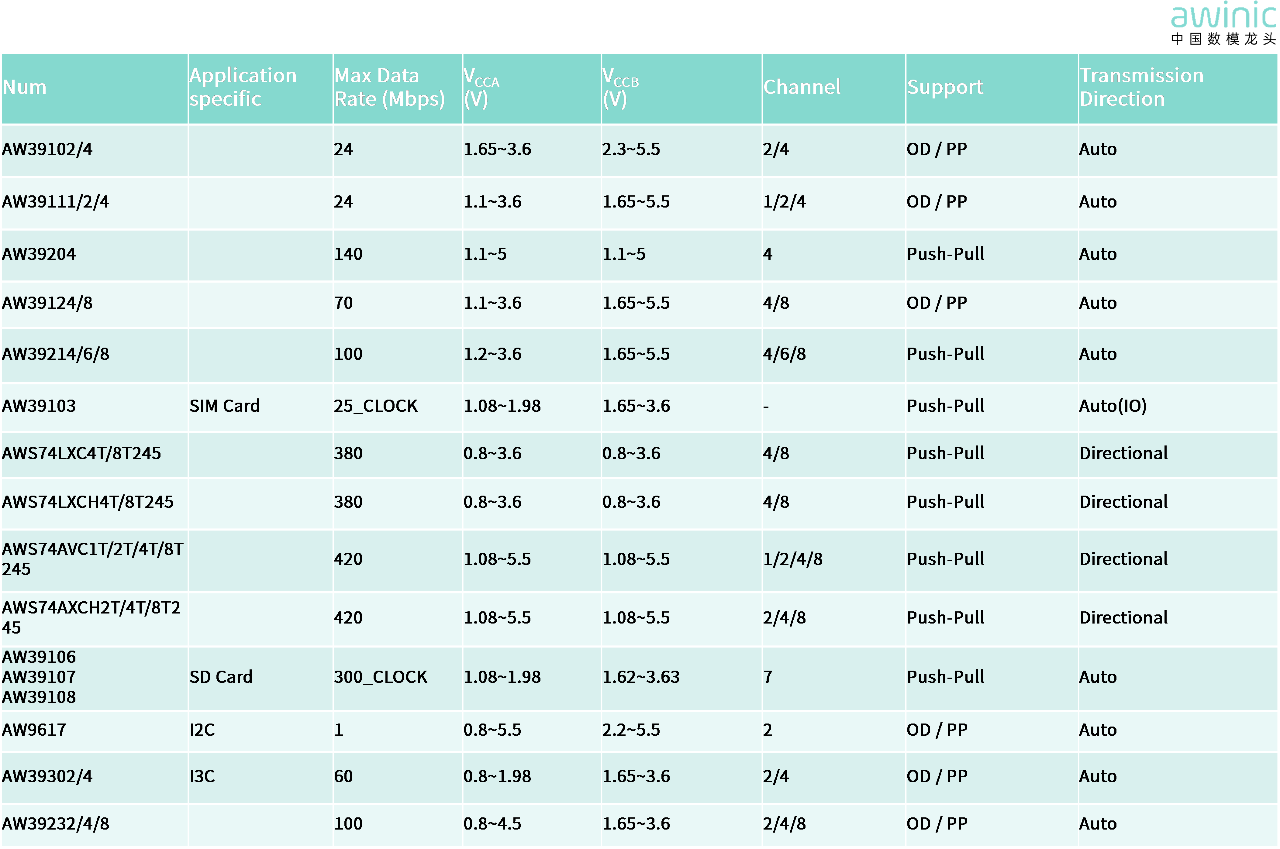
Appendix: Level Translator Product Portfolio