In portable devices such as mobile phones,every square millimeterof internal space can be described as“prime real estate”. With the proliferation of5G, multi-camera systems, large batteries, and cooling solutions, smartphone manufacturers have matured in employing dual-function speaker units, i.e., using one speaker unit to perform two tasks. Through circuit switching and acoustic chamber design, it can bothoutput high-power loudspeaker playbackandmeet private call requirements. The direct benefit of this design is space saving. However,“hardware reduction”does not equal“performance reduction”. Compressing two operating modes with power differences of several times onto a single unit poses severe challenges for acoustic design, power management, and signal switching:
Vast power dynamic range: In loudspeaker mode, output power can reach1W~2W(driving8Ω/6Ωload), with transient peaks reaching6W~7W, whereas receiver mode requires only about0.3W~0.5W(driving16/24Ωload).
Dramatically increased noise sensitivity: The signal amplitude in receiver mode is lower than in loudspeaker mode, making it extremely sensitive toDClassPWMamplifier carrier, power supply ripple, and ground noise, easily resulting in“buzzing”background noise.
Switching transient shock: When switching between loudspeaker/and receiver modes,MOSFETcharge injection may generate“popping”sounds, affecting user experience.
It is precisely against this background that awinic initiated exploration intosimplerandmore reliableswitching solutions——From external discreteMOSFETto integratedSPSTanalog switches, aiming to elegantly solve power mismatch and switching noise issues with a singlelow-distortion,high-voltage-toleranceanalog switch.
AW35331FDRKey characteristic parameters
-
Signal voltage range:-20V~20V, capable ofFar exceeds its own supply voltage(2.3V~5.5V) andSupports negative voltage transmission
-
Ultra-low on-resistance: Typical value90mΩ,Excellent flatness (less than1mΩ), suitable forHigh-fidelity audio signal applications
-
Supports1.2V IOLogic level, facilitating low-voltageGPIODirect drive
-
SupportsPower-down protection,VCC=0VWhen , the switch path remains in a high-impedance state, isolating±20VVoltage
-
SupportsHigh current, ensuring continuous overcurrent capability >1.5A, with peak current reaching2.5AOr more
AW35331FDRTypical Application Diagram
-
AW35331Normal application requires onlyOneVCCFiltering capacitor.
-
ENThe pin itself has no internal pull-up or pull-down resistors. If externalGPIOIs used for control, it is recommended to reserve a weak pull-down resistor externally,KΩOrMΩMagnitude is acceptable, to ensureGPIOHas a stable state when in high-impedance mode; to preventENPin from external high-frequency signal interference, it is recommended to reserve aENFiltering capacitor.0.1μFFig.
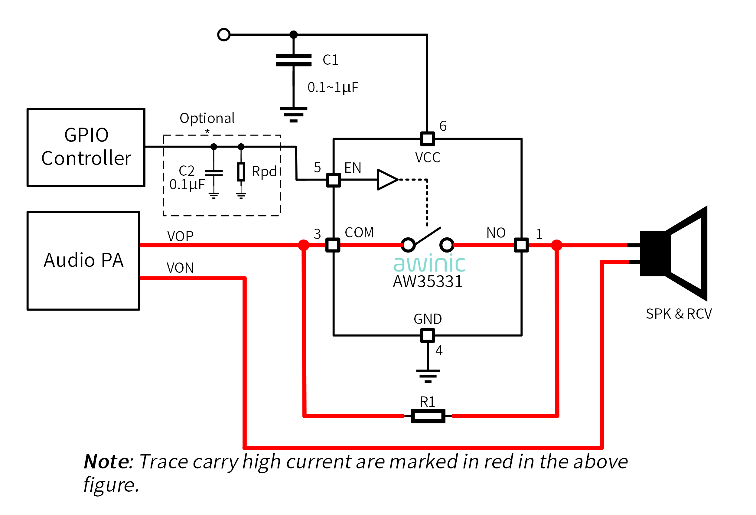
Typical Application Diagram1 AW35331FDRThe size of awinic is
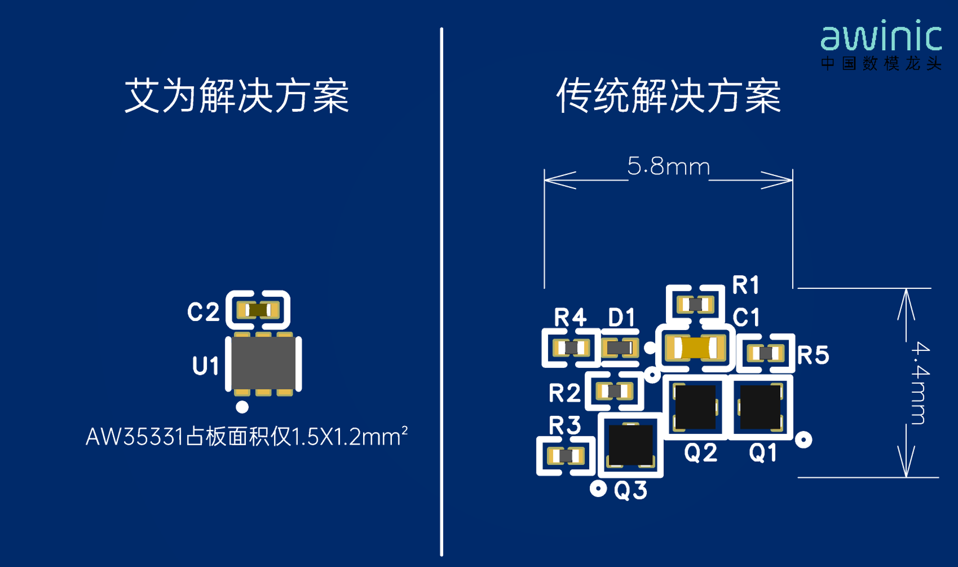
AW35331FDR, requiring only one filtering capacitor externally. Compared to traditional discrete component solutions, the number of components is directly reduced fromDFN-6L 1.5mm × 1.2mm × 0.4mmThe originalComponents to10Components2,And the board area occupation is also reduced fromPCBTo less than25.52mm², saving board area by3mm². (Actual results depend on specific project stacking)88%
Figure2 PCBDevice and Area Proportion Comparison
Main Advantages of This Solution
In practical applications of audio links, issues often arise due toparasitic effects, for instance, on actual circuit boards (PCB), where parasitic inductance and capacitance exist, resulting innegative overshoot voltagethat cannot be avoided. During this process, the switch must ensure lossless signal transmission to the subsequent load, without causing clipping due to the inability to transmit negative voltage.AW35331Supportspositive and negative voltage transmission, effectively avoidingclipping issueson the audio link, thereby preventing the generation of noise.
The switch, located in the audio path, needs to handle rapidly changingPWMmodulated waves. To achieve goodTHD+Nperformance, a fast dynamic response and maintenance of constant on-resistance are requiredRON, ensuring△RONminimal deviation across the full swing range. For power transistors, it is necessary to maintain the power transistorVGSconstant. awinic adopts aCharge pumpstructure, which achieves constant switch on-resistance by sampling the voltage at the source of the back-to-back configuration in real time and superimposing a fixed voltage on it to ensure the constancy of theNMOSvoltage.VGSvoltage to achieve constant switch on-resistance.
Derived Application Solutions
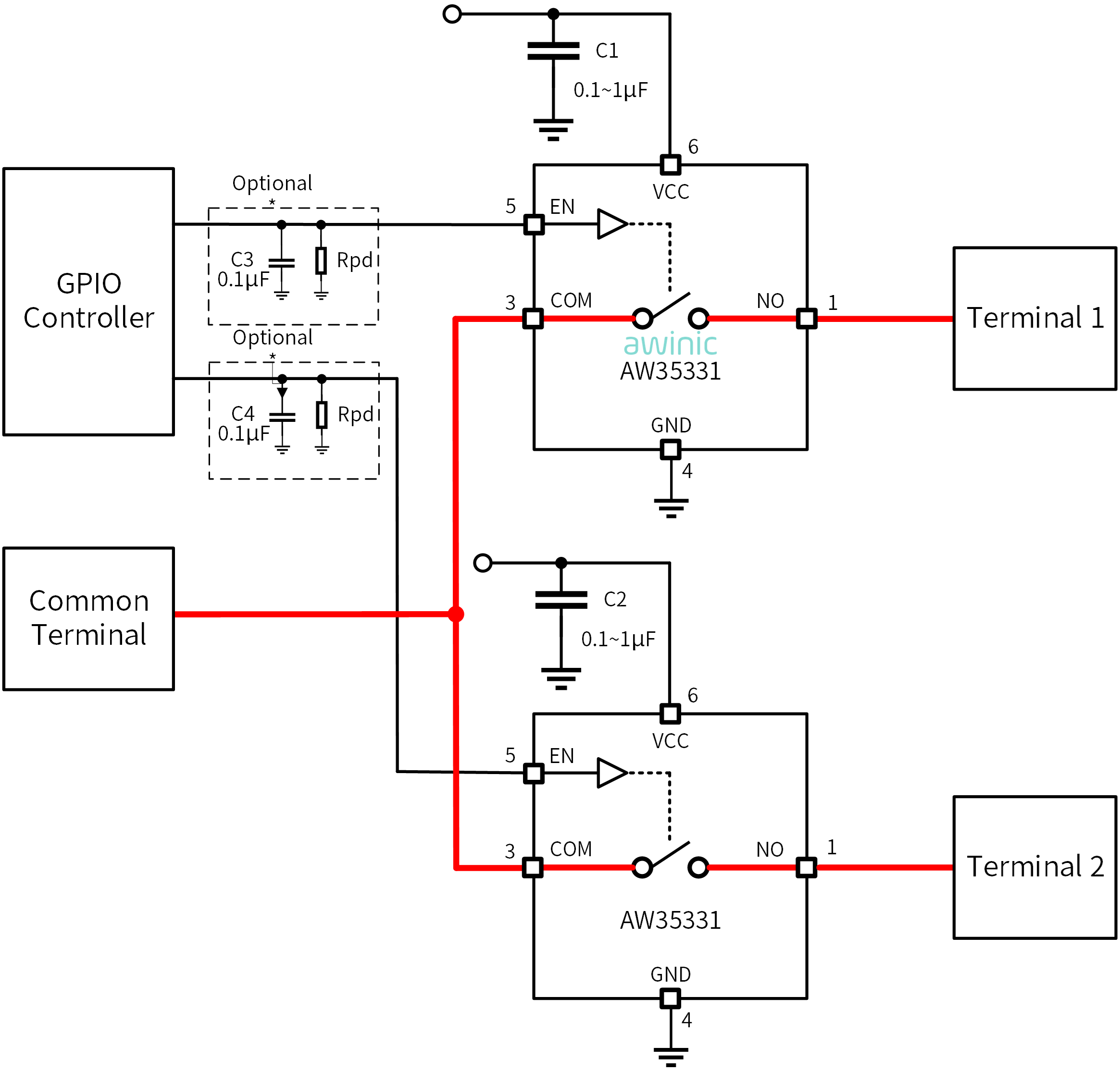
AW35331FDRWith its excellent performance, it can also be applied indual-device parallel application scenarios. Using2devicesAW35331FDRcan implementSingle-Pole Double-Throw (SPDT)SPDTfunctionality, used fortransmitting positive and negative voltage signals or for high-current applications. The application block diagram is as follows:
Figure3 DualAW35331Parallel Implementation forSPDTApplication