With the rapid
iteration of artificial intelligence, cloud computing, big data, and edge AI
technologies, the global server industry has entered a new cycle of high
growth. In 2026, the year-over-year growth rate of global server shipments is
expected to reach 12.8%. Benefiting from the surge in demand for AI training
and inference scenarios, the shipment growth rate of AI servers will exceed
28%. This growing demand continuously escalates the requirements for solution
stability and power consumption control. Following this industry trend, AWINIC
Technology has launched a comprehensive server solution covering three major
product series: I²C interface, power management, and signal chain, providing
high-performance, high-reliability domestic chip options for servers.
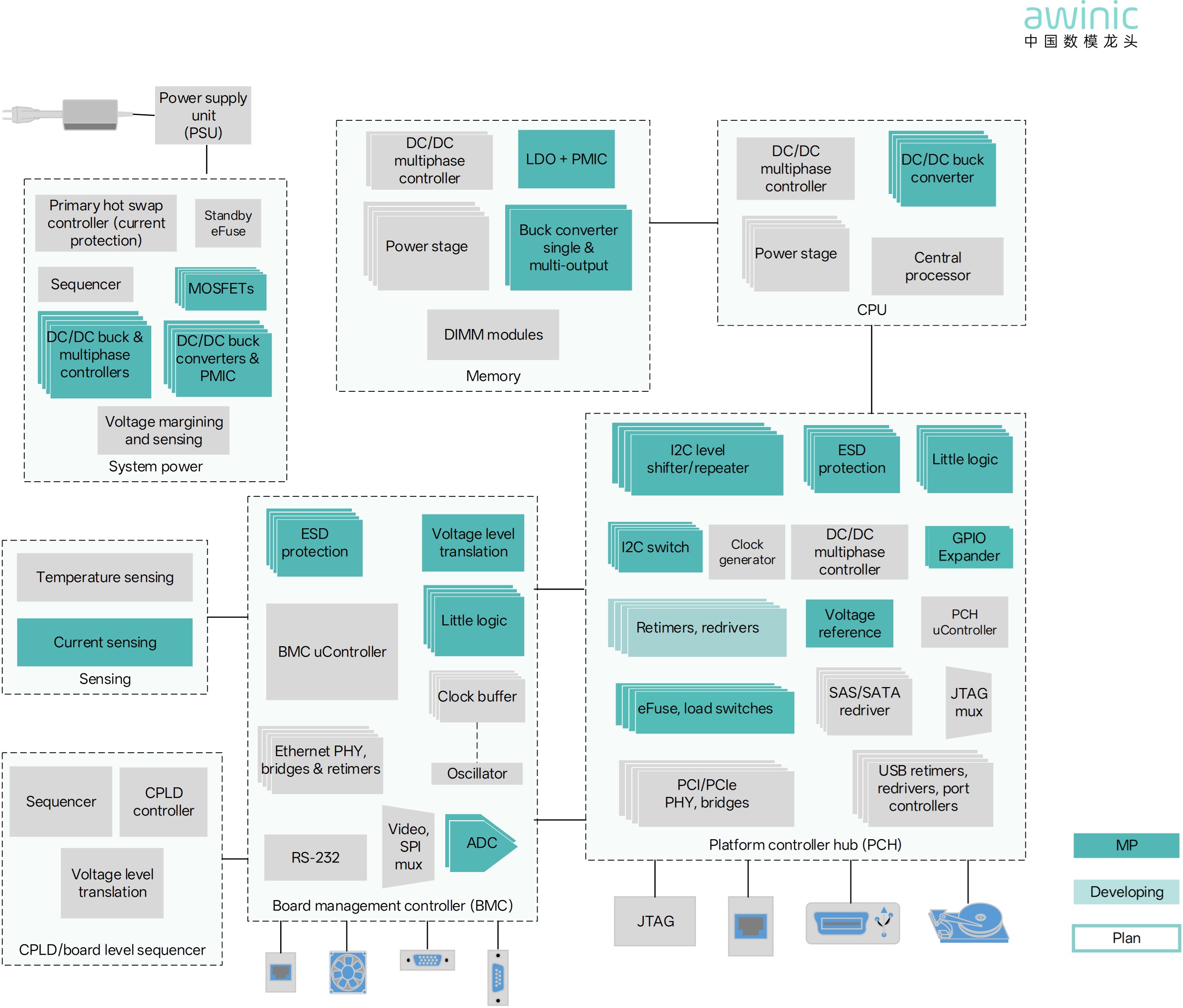
Figure 1 Server
Application Block Diagram
1. Three Major
Product Series
01 I²C Interface
Series
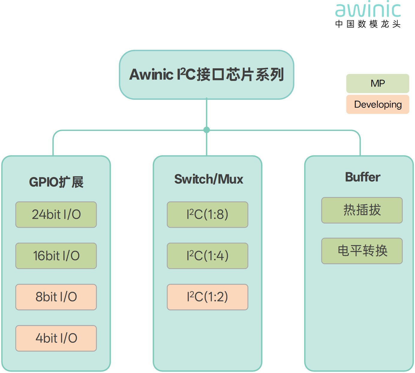
Figure 2 AWINIC
I²C Interface Chip Series
AWINIC's I²C
interface series includes three product subcategories:
-
I²C
GPIO Expander: Saves host I/O pins, simplifies layout and routing, reduces system
cost
-
I²C
Switch:
Extends I²C bus, resolves I²C address conflicts
-
I²C
Buffer:
Extends I²C bus, provides segmented bus isolation, hot-swap bus buffering,
and bidirectional level shifting
1. AW95124:
24-bit GPIO Expander
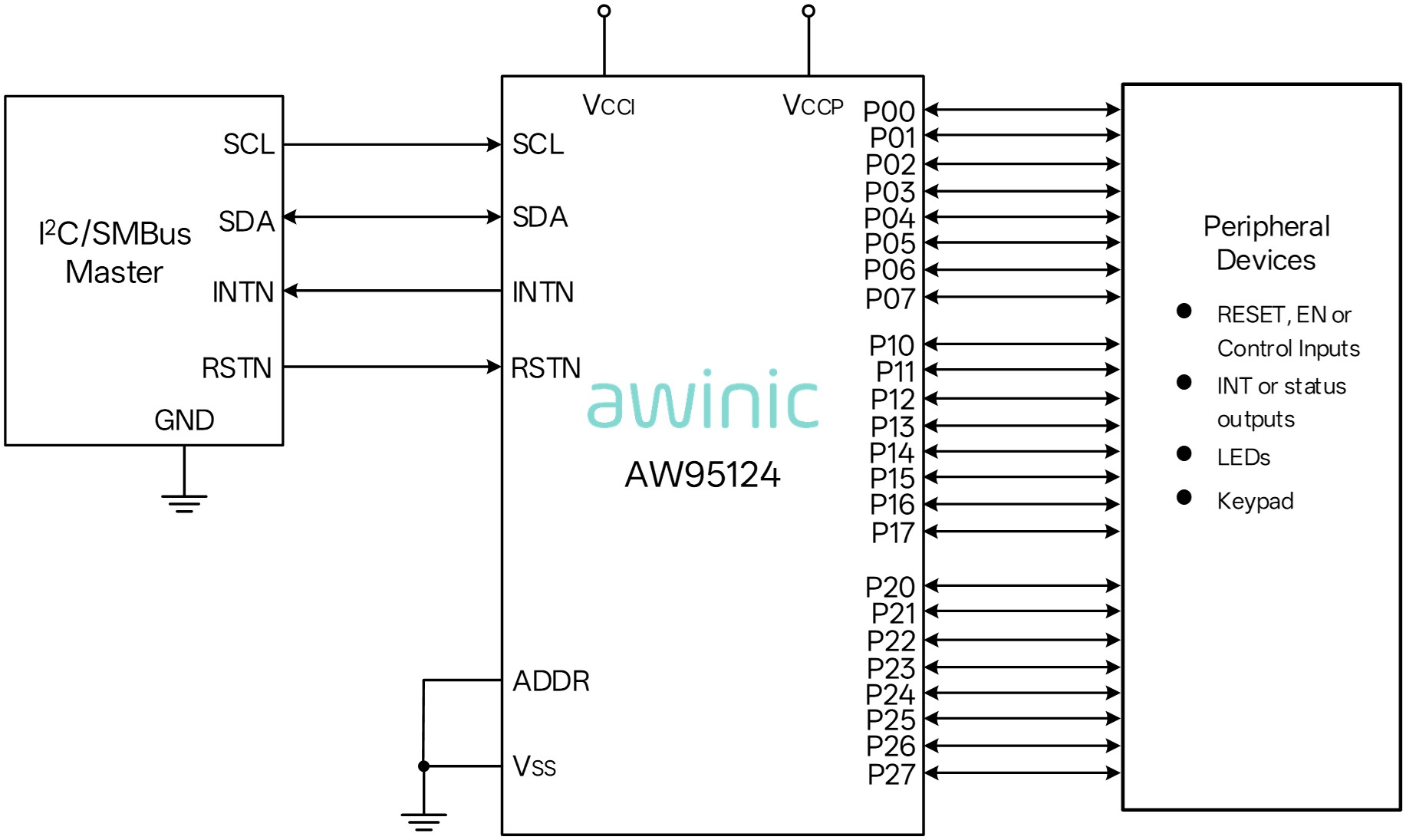
Figure 3 AW95124
Application Diagram
-
24-bit
GPIO parallel port expander
-
1MHz
I²C, SMBus compatible
-
Level
shifting function, VCCI/P input range: 1.08V ~ 3.6V
-
Interrupt
output (active low)
-
Expandable
I²C address, supports up to 4 devices
-
Package:
QFN 5mm × 5mm -32L
2. AW9548: I²C
Bus Switch
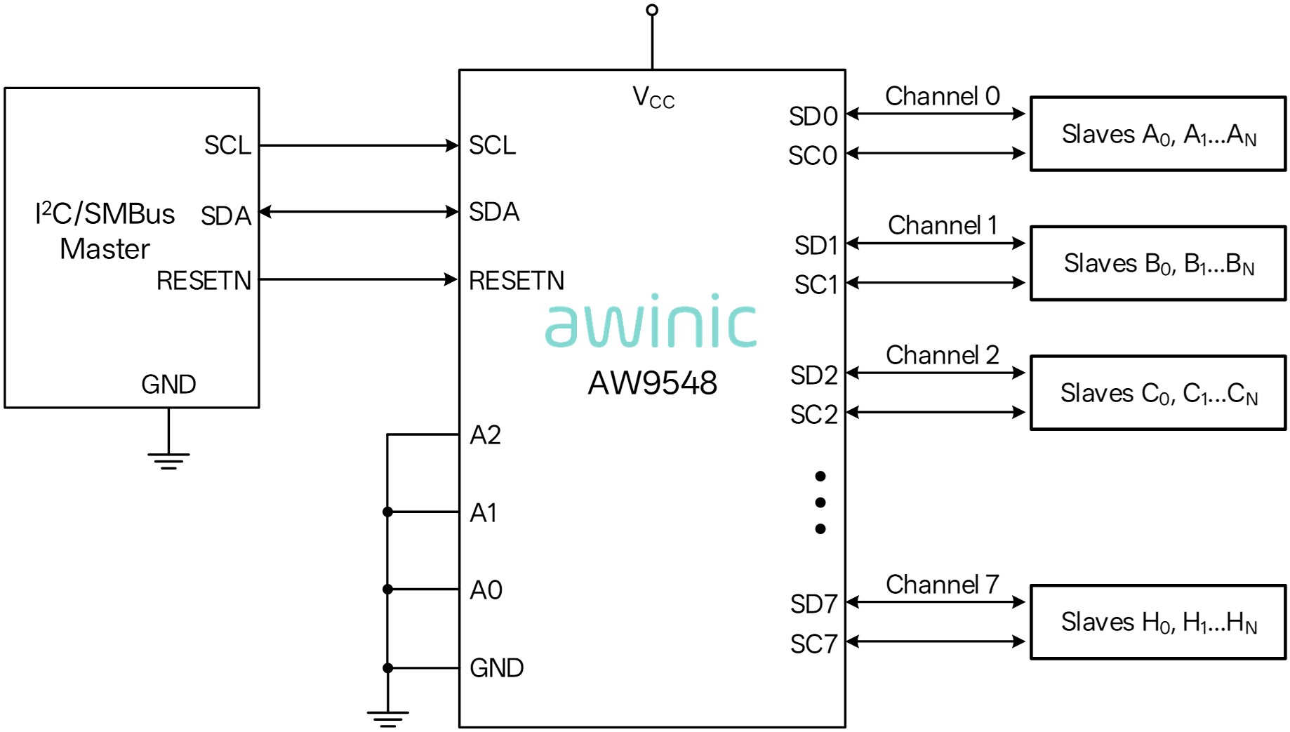
Figure 4 AW9548
Application Diagram
-
1:8
channel bidirectional translation switch
-
400kHz
I²C, SMBus compatible
-
VCC
input range: 1.65V ~ 5.5V
-
3
I²C address expandable pins, supports up to 8 devices
-
Supports
hot-swap, no glitch during power-up
-
1μA
low standby current
-
Packages:
-
AW9548:
TSSOP 7.80mm × 4.40mm -24L, QFN 4mm×4mm-24L
-
AW9546:
TSSOP 5mm × 4.4mm -16L
3. AW9617: I²C
Bus Buffer
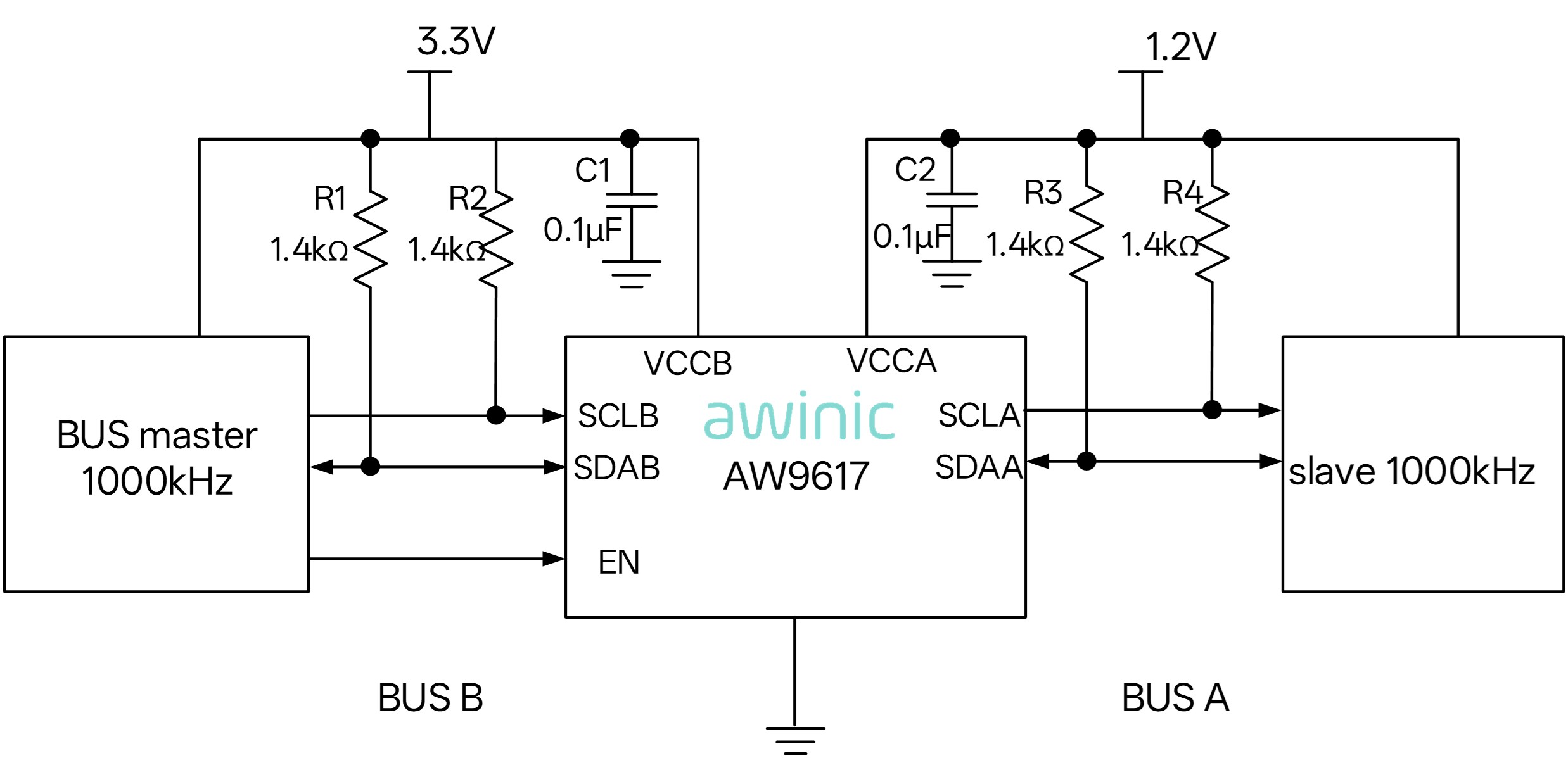
Figure 5 AW9617
Application Diagram
-
Supports
bidirectional level shifting and transmission of I²C bus signals
-
A-side
voltage range: 0.8V to 5.5V
-
B-side
voltage range: 2.2V to 5.5V
-
1MHz
I²C, SMBus compatible
-
Load
capacitance: 540pF @ 1MHz I²C, 4000pF @ 400kHz I²C
-
Active-high
enable
-
Supports
clock stretching and multi-master arbitration
-
Package:
MSOP 3.0mm × 3.0mm -8L
02 Power Management
1. AW35141A: 6A
Load Switch
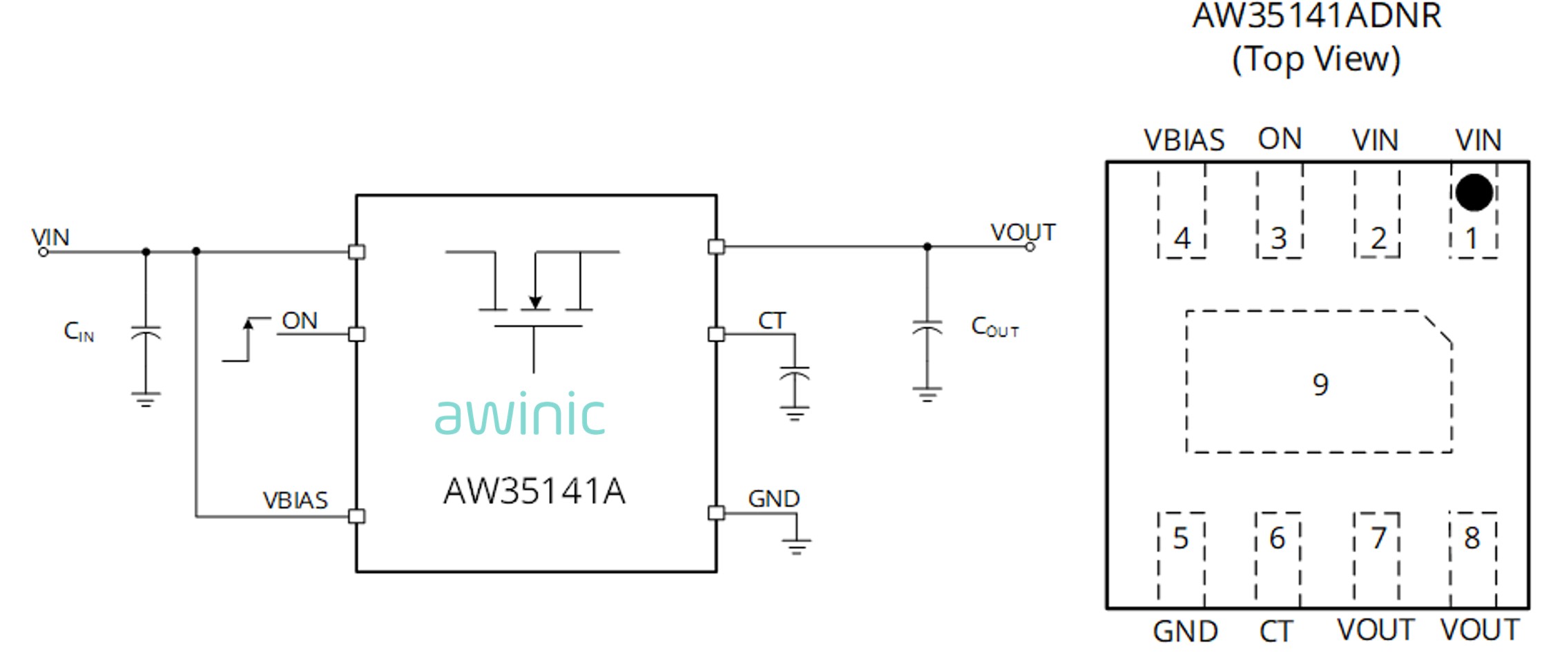
Figure 6
AW35141A Application Diagram
-
Input
voltage: Vbias = 2.5V ~ 5.5V, Vin = 0.6V ~ Vbias
-
Load
current: 6A
-
Quiescent
current: 20μA @ 3.3Vin
-
Rdson
= 19mΩ @ 3.3Vin
-
Ten
= 980μs, Tr = 560μs
-
QOD
function
-
Package:
DFN-8L 2mm×2mm×0.75mm
2. AW35019A:
5V/3A eFuse
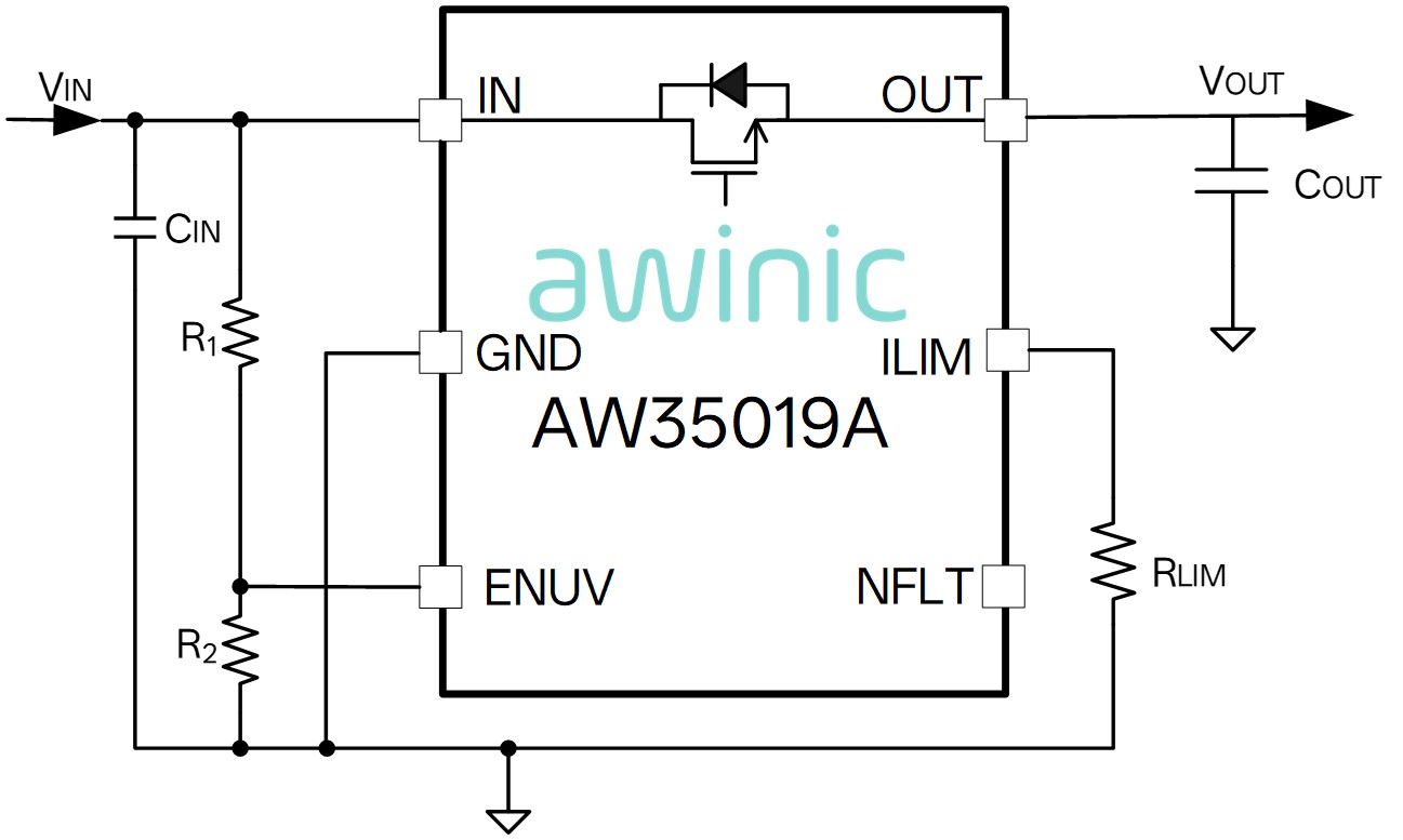
Figure 7
AW35019A Application Diagram
-
Input
voltage range: 2.7V ~ 6.5V, input withstand voltage: 24V
-
Power
MOSFET on-resistance: 50mΩ
-
Configurable
current limit range: 250mA ~ 3A
-
Current
limit accuracy: ±7%
-
Input
overvoltage protection: 7.5V threshold, 150ns response time
-
Output
clamp voltage: 5.4V (5.4V < VIN < 7.5V)
-
Other
protection features: soft-start, thermal shutdown, Fault interrupt
indicator
-
Package:
DFN 2mm×2mm×0.75mm-6L
3. AW37023:
5V/3A LDO
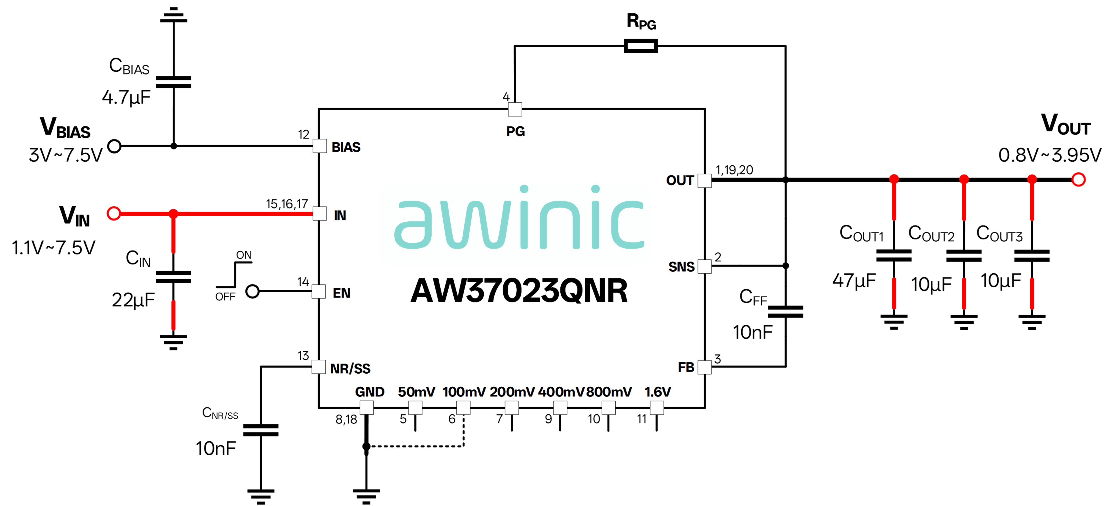
Figure 8 AW37023
Application Diagram
-
Input
voltage range: 1.1V ≤ VIN < 7.5V, with bias
-
Output
voltage range: 0.80V ~ 5.2V (FB config mode), 0.80V ~ 3.95V (IO config
mode)
-
Low
dropout: 180mV (Max.) @ 3A
-
Low
output noise: 5μVrms @ 0.8V output, 11μVrms @ 5.0V output
-
Open-drain
Power-Good signal
-
Protection
features: current limit, thermal shutdown
-
Package:
QFN 3.5mm×3.5mm-20L
03 Signal Chain
Series
1. AW39128:
8-bit Level Shifter
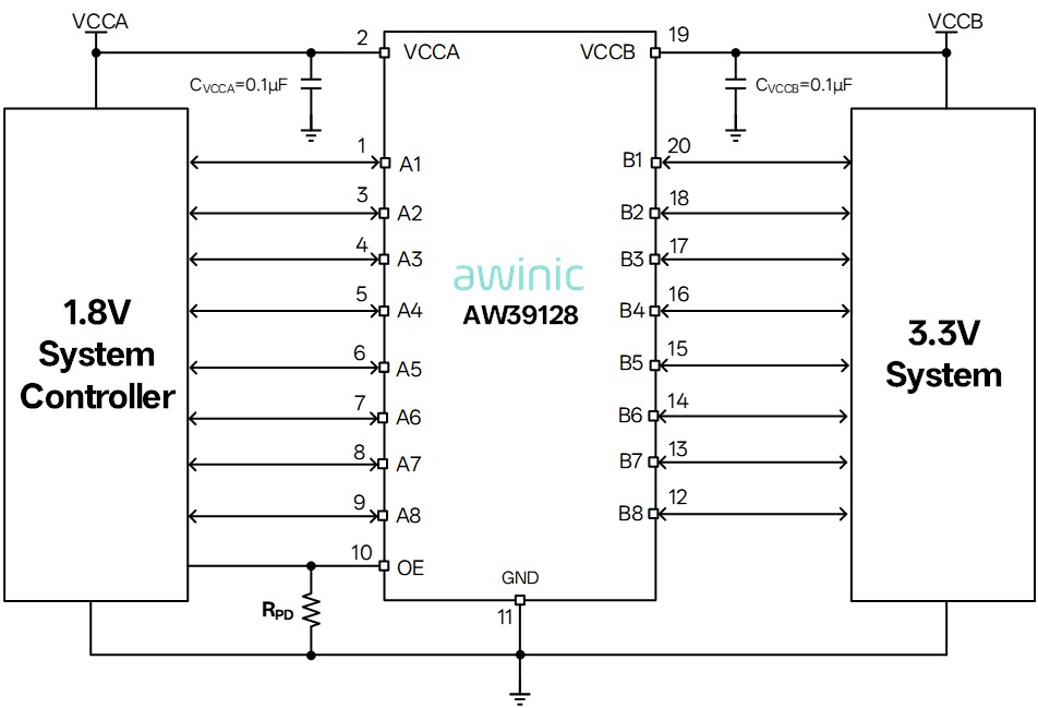
Figure 9 AW39128
Application Diagram
-
Auto-direction
sensing for signal transmission
-
Maximum data rates:
-
70Mbps
(Push Pull)
-
2Mbps
(Open Drain)
-
Voltage range:
-
A-port
and VCCA: 1.1V ~ 3.6V
-
B-port
and VCCB: 1.65V ~ 5.5V
-
VCCA
≤ VCCB
-
Integrated
pull-up resistors on A-port & B-port
-
VCCA
/ VCCB arbitrary power-up/power-down sequencing
-
ESD protection:
-
ANSI/ESDA/JEDEC
(A-port): ±4kV HBM; ±1kV CDM
-
IEC
61000-4-2 ESD (B-port): ±6kV contact; ±8kV air
-
Package:
TSSOP 6.5mm×4.4mm-20L
2. AWS74LVC1G17:
Single Schmitt-Trigger Buffer
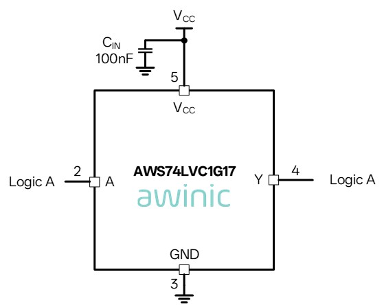
Figure 10
AWS74LVC1G17 Application Diagram
-
VCC
range: 1.65V to 5.5V, input voltage up to 5.5V
-
IOFF
supports partial power-down mode
-
tpd:
3.7ns @ 3.3V
-
High
output drive: ±24mA @ VCC = 3.0V
-
Operating
temperature range: -40°C to 125°C
-
Package:
SOT353 - 5L
2. Server
Solution Product List
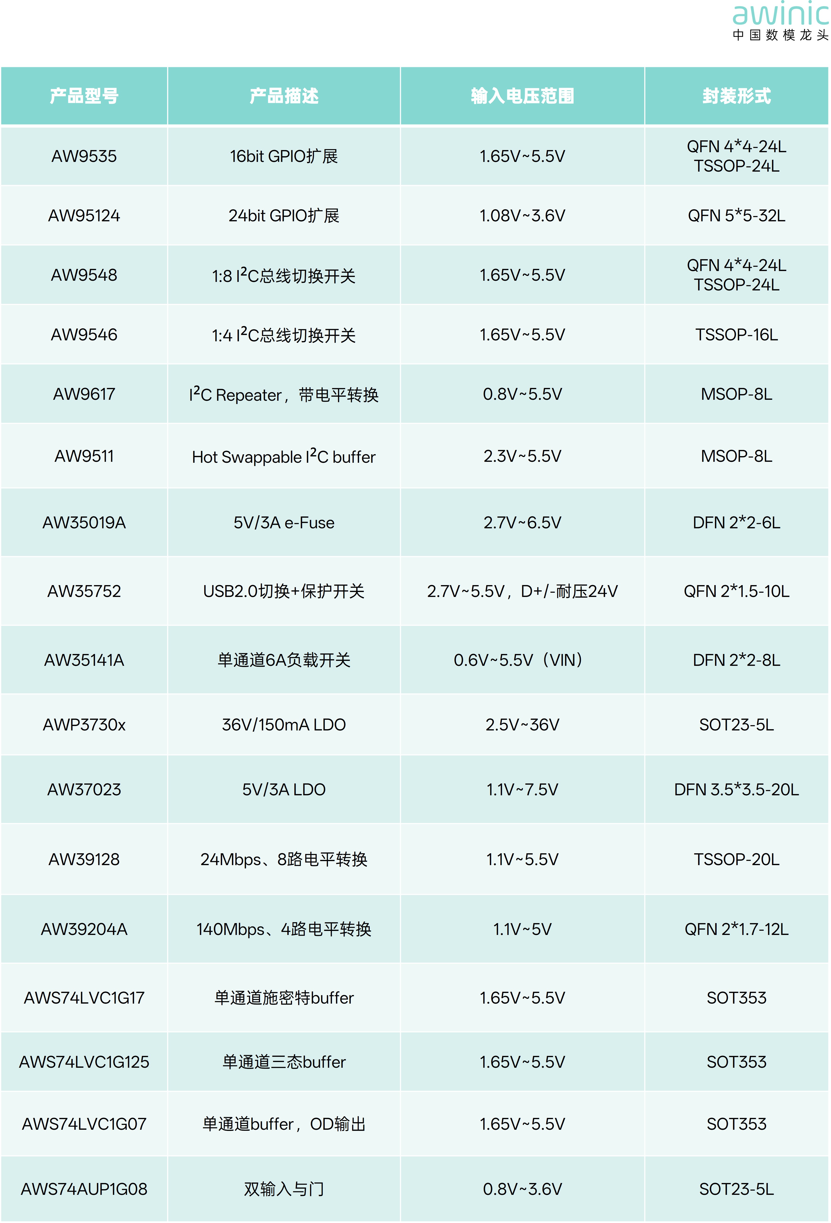
Table 1 AWINIC
Server Solution Product Recommendation Table
Conclusion
As a leading
domestic company in analog-mixed signal, power management, and signal chain
chips, AWINIC Technology has深耕 the analog chip
field for many years. Targeting typical server application scenarios, the
company has developed a highly reliable, highly integrated complete solution
covering I²C interface, power management, and signal chain. This solution meets
server requirements for I²C bus expansion, low-voltage power protection and
conversion, and low-speed signal processing, helping customers achieve
performance upgrades and domestic substitution.

 EN
EN


