In recent years,
flagship smartphones have continuously stacked large-size sensors and
multi-camera modules in pursuit of high image quality, leading to a significant
increase in device thickness (for example, the Xiaomi 15 Ultra compromised on
thickness due to its telephoto module). Meanwhile, although the
algorithm-driven computational photography has enhanced convenience, excessive
retouching has led users to miss the "authentic optical texture." The
dual user demand for a "slim, lightweight feel" and "professional-grade
imaging" has given rise to a new solution: hardware expansion through a magnetic
telephoto converter lens, avoiding excessive bulkiness in the phone body.
The telephoto converter lens provides pure physical optical enhancement,
catering to professional users' pursuit of authentic light and shadow.
The
following diagram illustrates AWINIC's telephoto converter lens solution:
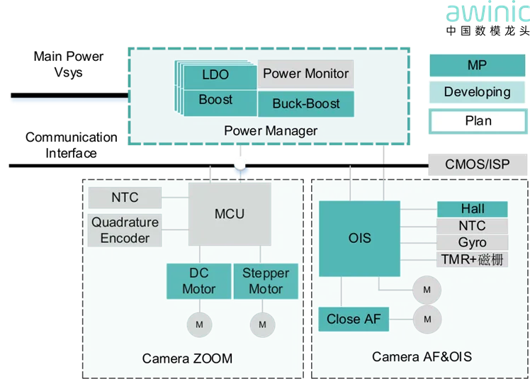
Figure 1:
Telephoto Converter Lens Application Block Diagram
External lenses are generally heavy and require a long
travel distance for OIS/AF, necessitating the use of a motor driver chip. Since
AWINIC launched its VCM motor driver ICs in 2020, its OIS/AF control solutions
have been highly acclaimed, becoming the preferred choice for VCM motor control
among many mainstream domestic and international manufacturers.
AWINIC has introduced the high-precision,
three-channel driver AW86068CSR to meet the OIS/AF control requirements of
telephoto converter lenses:
· Memory: 64KByte Flash Memory, 32KByte SRAM
· Development: Provides SDK, supports customer secondary
development and integration of AWINIC control solutions
· Interface: 12.5MHz I3C high-speed communication interface
· ADC: 3x 16-bit high-precision ADC
· Power: VM = 1.5V to 3.6V, supports dynamic voltage scaling
· Package: WLCSP 3.555mm x 1.255mm x 0.3mm-27B
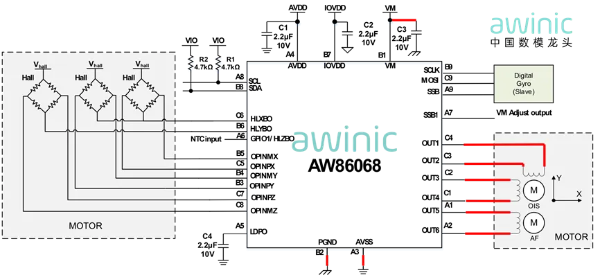
Figure 2: AW86068CSR
Typical Application Schematic
In telephoto converter
lens solutions, there is often an AF axis requiring a long travel distance,
which is well-suited to our long-stroke, high-voltage closed-loop control
chip, the AW86026HCSR:
· Power: 1.7V to 5.25V,
dynamic voltage scaling
· Control: Integrated AWINIC
2nd+ generation high-performance closed-loop control algorithm, featuring
electronic damping, SmartHolding, and other characteristics
· Hall Sensor: Integrated
high-precision Hall sensor
· Drive Current: Default
±300mA drive current
· ADC: 16-bit
high-precision ADC
· Package: WLCSP 1.5mm x
0.86mm x 0.265mm-6B

Figure 3: AW86026HCSR Typical Application
Schematic
In Camera ZOOM applications, the AWD86307DNR DC motor driver chip is
used to drive the zoom DC motor. It achieves smooth start/stop, fast
response, and low-noise zooming through PWM and current control.
The AW86426FBR
stepper motor driver chip is used to drive the zoom or
focus stepper motor. It supports micro-stepping control and precise
positioning, ensuring stable lens position and high repeatability.
AW86307DNR Features:
·
VDD Voltage Range: 0V - 12V
·
VCC Voltage Range: 1.8V - 5.5V
·
RDS(ON) HS + LS: 950 mΩ
·
Maximum Output Current: 1.1A
·
Maximum Sleep Current: 120 nA
·
Independently controlled nSLEEP pin
·
Short-Circuit Protection
·
Over-Temperature Protection
·
Under-Voltage Lockout Protection
·
Package: DFN 2mm x 2mm x 0.75mm-8L

Figure 4: AW86307DNR Typical Application
Schematic
AW86426FBR Features:
·
Operating Voltage: DC 3.0V ~ DC 12V
·
Maximum Drive Current: 1.1A
·
Ultra-Compact Package: FCBGA 2.4mm x 2.0mm x 0.59mm-30B
·
Rdson HS+LS: Typical 0.95Ω
·
Supports up to 1/32 Micro-Stepping
·
Supported Decay Modes:
o Adaptive
Decay Mode
o Mixed Decay
o Slow Decay
o Fast Decay
·
Programmable Overcurrent Shutdown Time:
o 10μs
off-time
o 20μs
off-time
o 30μs
off-time
·
Programmable Motor Torque
·
Short-Circuit Protection, Over-Temperature Protection, and
Under-Voltage Lockout Protection
·
Fault Condition Indication
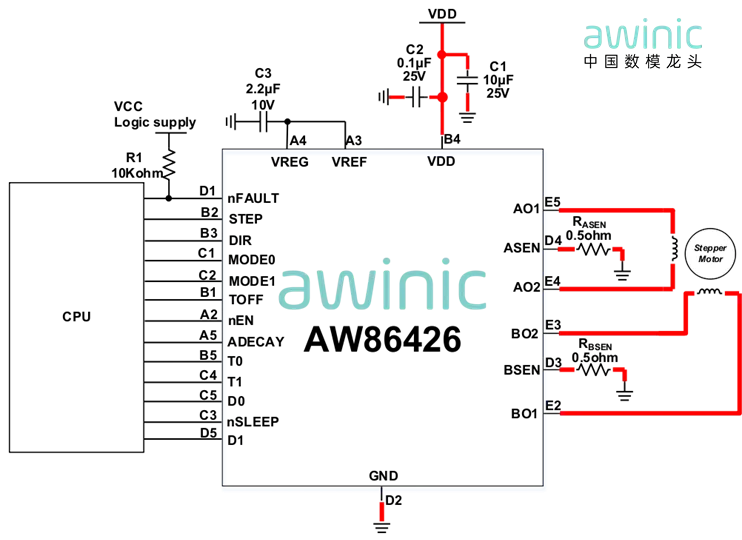
Figure 5: AW86426FBR Typical Application
Schematic
Additionally, to complement our dynamic voltage scaling
solution, the AWP37702CSR—specifically
designed by us for VCM dynamic voltage scaling—can be utilized:
· Input Voltage Range: 2.2V ~
5.5V
· Output Voltage Range: 1.4V ~
4.575V
· Ultra-Low Quiescent Current: 2.8 μA
· Ultra-Low Shutdown Current: 0.3 μA
· Dynamic Voltage Scaling Control: Supports
slew rates of 2V/ms, 5V/ms, 10V/ms, and 20V/ms
· Operating Modes: Automatic
PFM mode and forced PWM mode selection
· Interface: I2C
interface up to 1MHz (I2C supports 1.2V I/O levels)
· Maximum Continuous Output Current:
o Up to 0.8A
at VIN ≥ 2.2V, VOUT = 3.5V
o Up to 1A at
VIN ≥ 2.5V, VOUT = 3.5V
o Up to 1.5A
at VIN ≥ 3.3V, VOUT = 3.5V
· Package: WLCSP 1.3mm x
1.3mm-9B
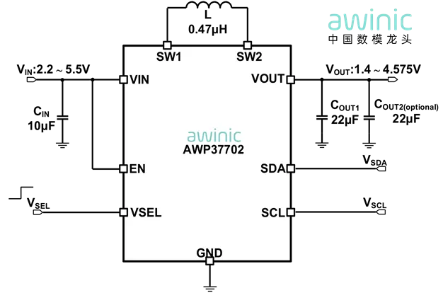
Figure 6:
AWP37702CSR Package Information
Furthermore, in
the power supply and battery management module, a multi-layer protection design
utilizing AWINIC products is implemented: the AW37030D110EDNR LDO chip provides
a 300mA high-performance regulated output to power core components; the AW33901FCR
over-voltage protection chip safeguards downstream circuits with its
30mΩ low on-resistance and 50ns fast shutdown characteristic.
Below is a
partial chip selection guide. For more chips, please visit the AWINIC official
website.
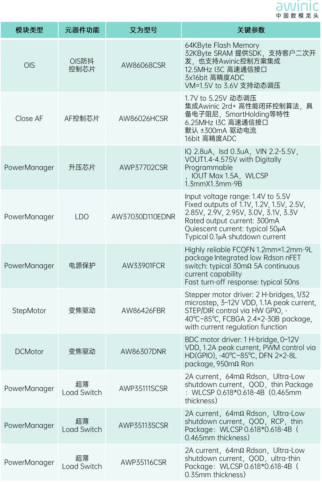
Table 7: Bill of Materials (BOM) Selection Guide


