With the rapid development of smart wearable devices and portable tools, battery life has become a core pain point in user experience. Are the increasing number of functional modules and high overall power consumption still limiting your product design? Does frequent charging reduce the practical value of your end devices?
China's leader in analog and digital, Awinic, introduces a breakthrough solution—the new generation of ultra-low power consumption, ultra-small size Buck-Boost chip is officially launched!
It not only redefines power management efficiency but also provides enduring and reliable energy support for wearable devices, portable tools, and various smart terminals with extreme energy consumption control and stable output. Whether the device is in standby, light load, or high load operation, it can maintain efficient operation with ultra-low power consumption, fully unleashing the product's battery life potential.
Product Advantages
Ultra-Low Quiescent Current, Exceptional Full-Range Efficiency: Ushering in a New Era of Efficient Energy Utilization
As portable electronic products continue to pursue longer battery life and smaller sizes, every joule of energy is crucial. Awinic's power management chips, specifically developed for low-power applications, deliver unprecedented energy efficiency with ultra-low quiescent current and exceptional efficiency, making them ideal for space- and power-sensitive devices.
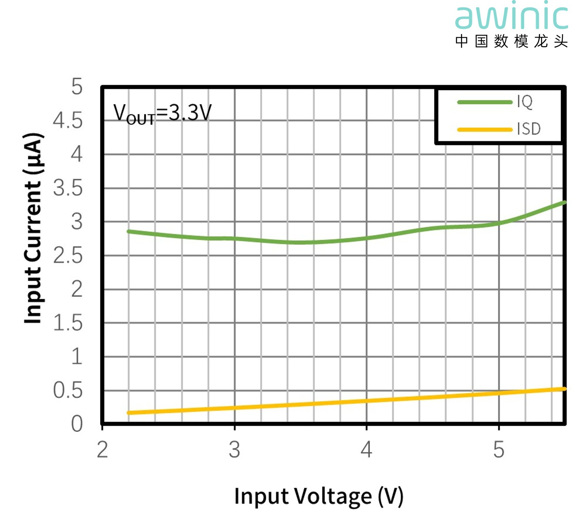
Figure 1 Input Current VS Input Voltage
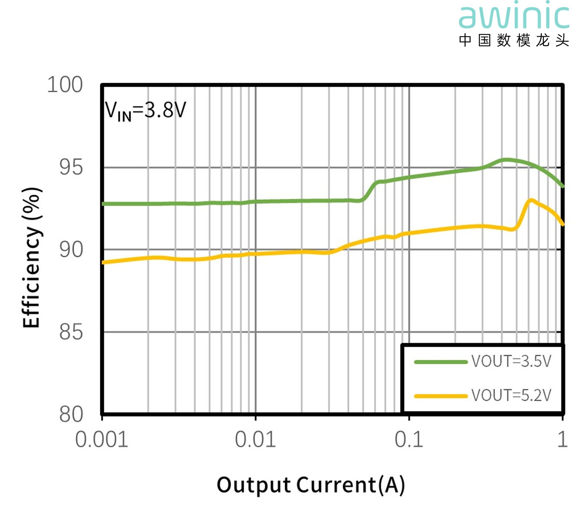
Figure 2 Efficiency vs Output Current
Excellent Dynamic Response Characteristics: Key to Ensuring Accurate PPG Measurement
In smartwatches, blood oxygen and heart rate monitoring based on the Photoplethysmography (PPG) principle involves emitting light through LEDs to the skin and receiving reflected light signals via photodiodes. This process requires low-frequency LED flickering, and each activation causes a sudden current surge, which can lead to voltage drops and noise, directly affecting signal acquisition quality. If the power supply response is slow, the LED activation time must be extended to stabilize the signal, increasing power consumption and limiting battery life.
Therefore, the transient response speed and stability of the power supply circuit are critical to PPG performance. Awinic's AWP37701Z power management chip, with its excellent dynamic response capability, stabilizes the output voltage within 10μs after a load transient, effectively suppressing voltage fluctuations and noise, and significantly improving the accuracy and reliability of PPG signal acquisition. This chip provides solid power support for high-precision, low-power blood oxygen and heart rate monitoring in wearable devices.
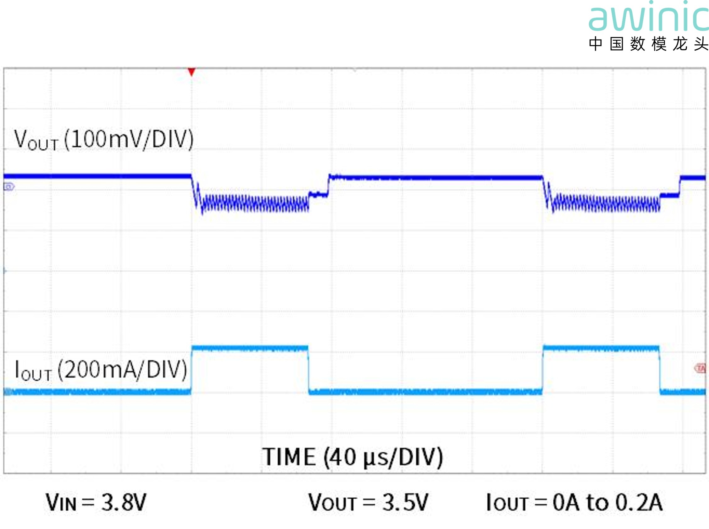
Figure 3 Load Transient
Seamless Smooth Mode Switching: A New Benchmark for Power Supply Stability in Wearables
-
Addressing the stringent stability requirements of battery-powered products, our newly launched Buck-Boost chip features an architecture design that enables seamless and smooth switching between Buck, Boost, and Buck-Boost operating modes. This chip completely resolves voltage step and oscillation issues that may occur during mode transitions in traditional power solutions, ensuring clean and stable power output across the entire input voltage range.
With its excellent mode-switching performance, this chip is widely applicable to various battery-powered electronic products, providing efficient and reliable power support for downstream circuits. It is particularly suitable for scenarios requiring absolute power stability under significant input voltage fluctuations, helping products achieve superior system performance.
AWP37701Z Product Introduction
-
Input Voltage Range: 2.2V ~ 5.5V
-
Output Voltage Range: 2.025V ~ 5.2V
-
Ultra-Low Quiescent Current: 2.8μA
-
Ultra-Low Shutdown Current: 0.3μA
-
Supports Dynamic Voltage Scaling Control (Slope: 1V/ms, 2.5V/ms, 5V/ms, 10V/ms)
-
Automatic PFM Mode and Forced PWM Mode Selection
-
I2C Interface up to 1MHz (I2C supports 1.2V I/O level)
-
Maximum Continuous Output Current:
-
VIN ≥ 2.2V, VOUT = 3.5V: IOUT up to 0.8A
-
VIN ≥ 2.5V, VOUT = 3.5V: IOUT up to 1A
-
VIN ≥ 3.3V, VOUT = 3.5V: IOUT up to 1.5A
-
Package: WLCSP 1.3mm x 1.3mm-9B
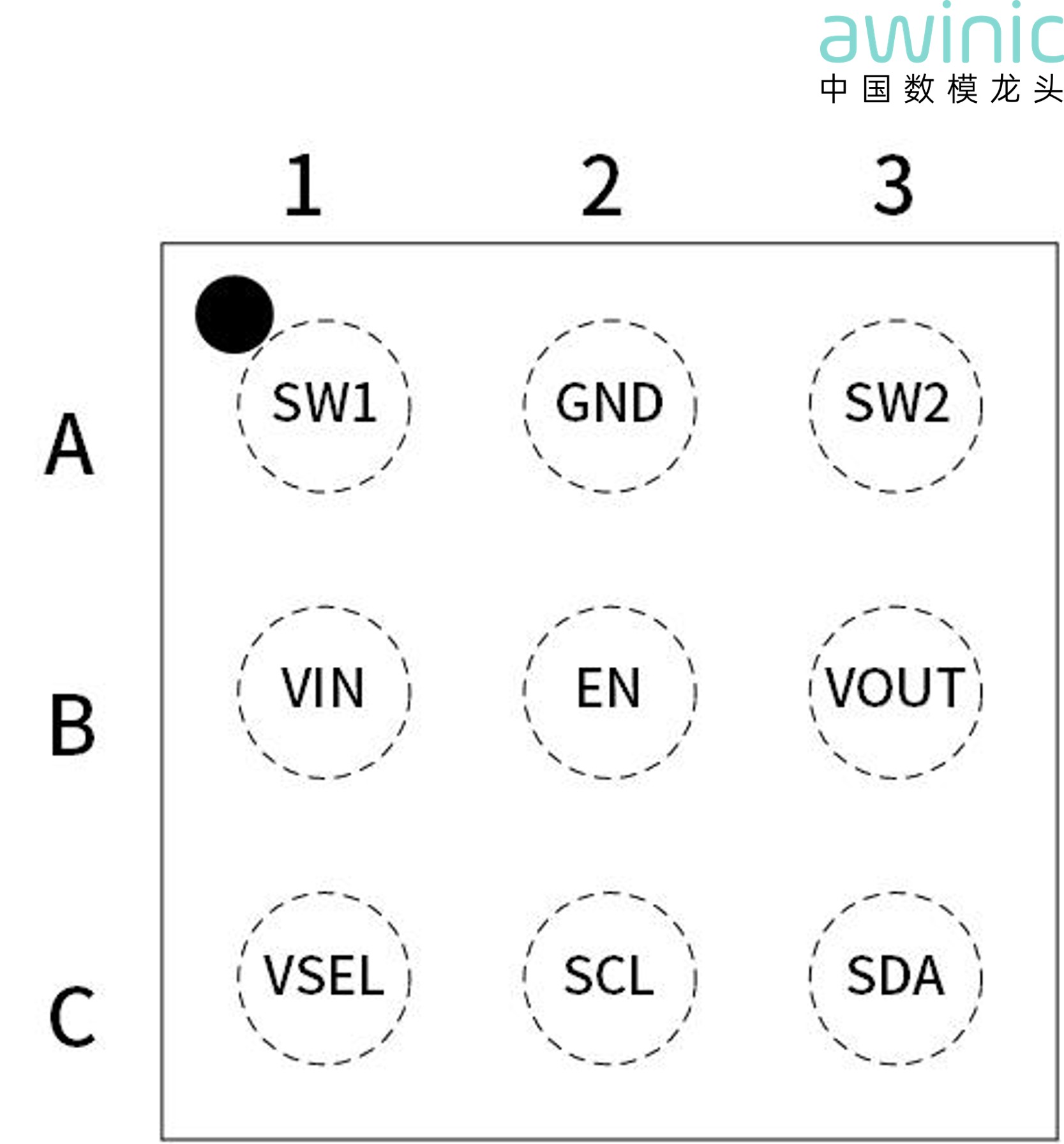
Figure 4: AWP37701Z Package Information
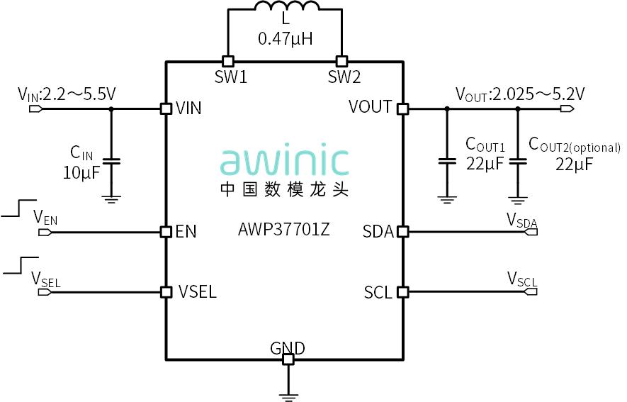
Figure 5: AWP37701Z Typical Application Diagram
Application Scenarios
Widely applicable to wearable devices, wireless earphone charging cases, smartphones, thermohygrometers, optical heart rate monitoring LED bias power supply, lithium battery or dual dry battery-powered products, and other applications with high requirements for power consumption, load transients, and size.
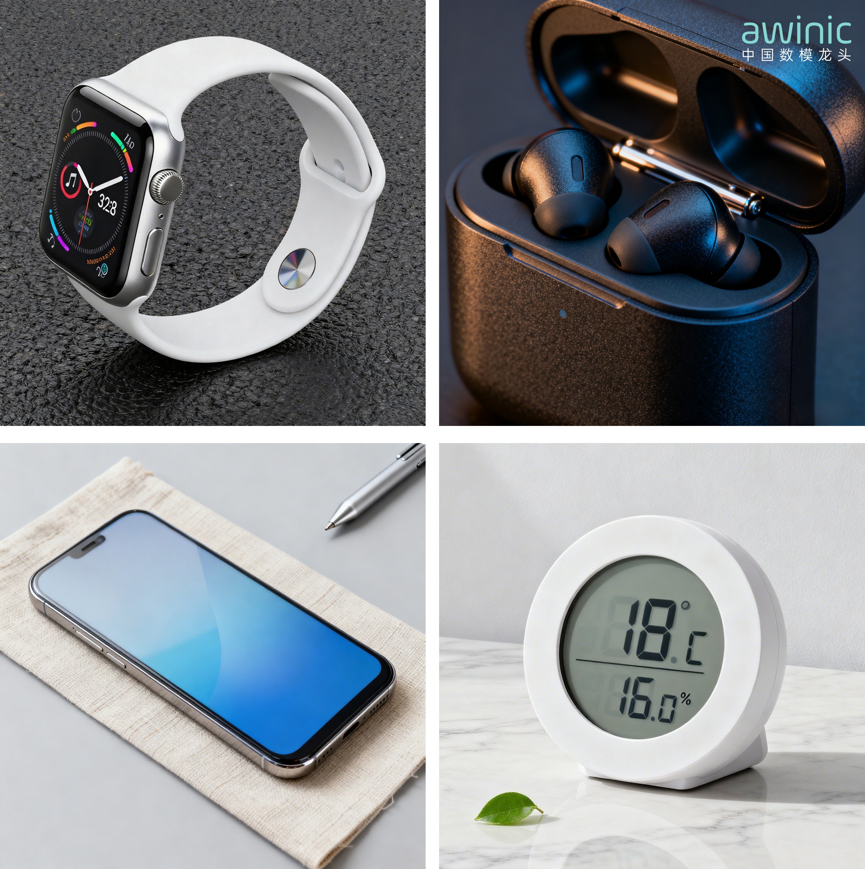
Figure 6: Application Scenarios
Product Selection Table
Buckboost
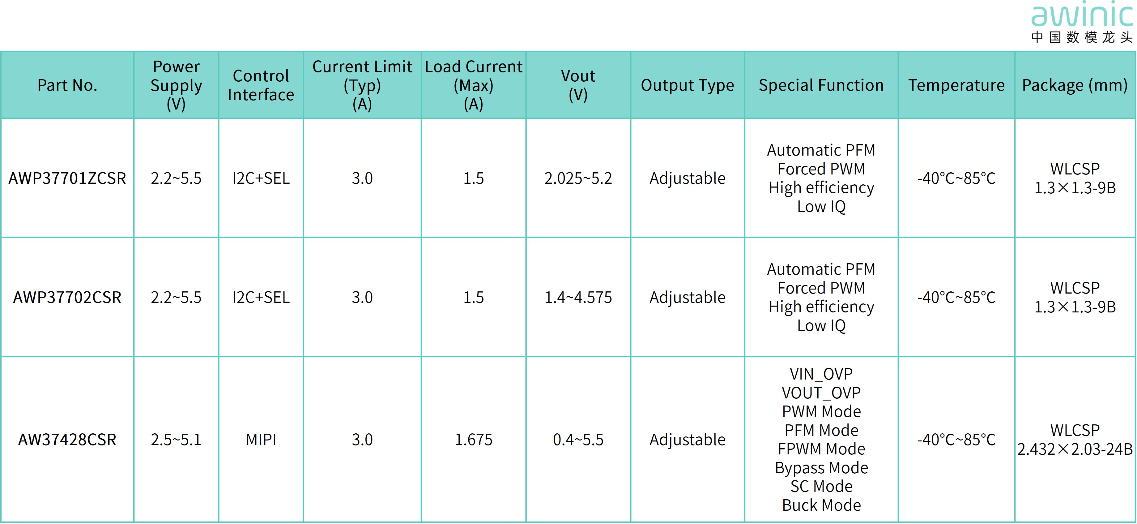
Table 1: Buckboost Product Selection Table
Buck

Table 2: Buck Product Selection Table
Boost
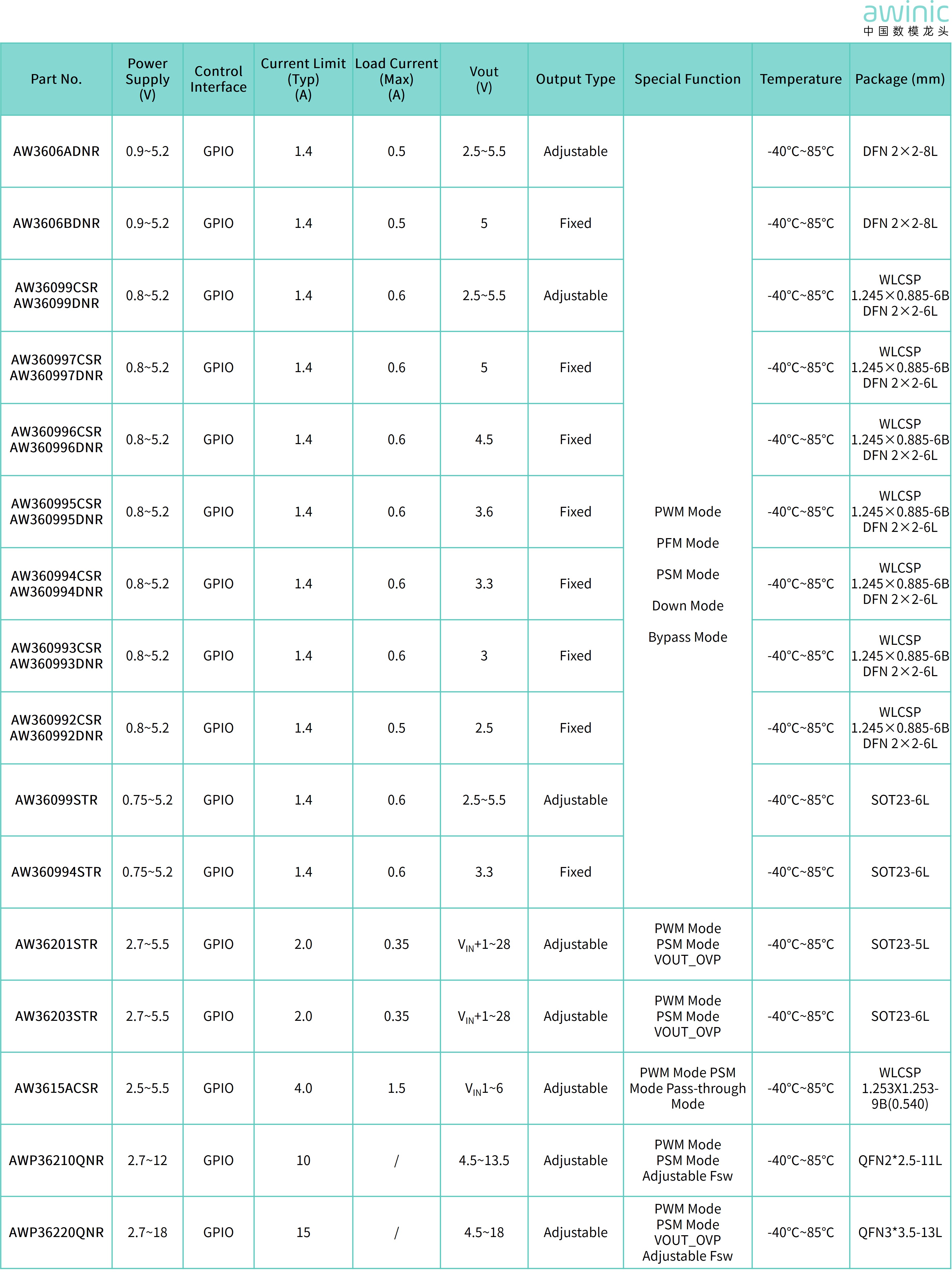
Table 3: Boost Product Selection Table


