On May 22nd, Xiaomi Technology released its new flagship
smartphone, the 15S Pro, which has attracted much attention. As a tribute to
Xiaomi's 15th anniversary, this phone features the self-developed "Xuanjie
O1 with second-generation 3nm process" flagship processor, which is the
biggest highlight. This news means that Xiaomi has taken a milestone step in
the field of core technologies. After years of technical accumulation and
strategic layout, Xiaomi has achieved a qualitative leap in chip research and
development, becoming the fourth global and second domestic mobile phone brand
to master core self-developed chips.
In response to the new platform's pursuit of extreme low
power consumption, it is reported that the "Xuanjie O1 3nm" SoC chip
adopts a 1.2V IO design. However, most of the current mainstream peripheral ICs
such as mobile phone baseband chips, camera modules, audio PAs, and motor
drivers still use 1.8V digital IO ports. To realize signal communication
between the main platform and peripherals, level conversion chips are needed to
convert the level signals output by the main platform to adapt to the level
standards of the peripherals. The technical adaptation of this link will be the
key to ensuring the coordinated work of the new platform and peripheral
components.
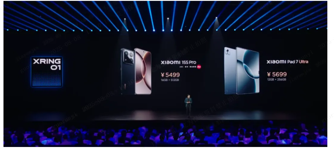
Picture 1 Xiaomi
15S Pro
AWINIC has been deeply engaged in the signal chain
product line for many years, among which the level conversion chip has a
long-term layout. This series of products is rich and diverse, covering various
specifications such as 2-channel, 4-channel, 6-channel, and 8-channel. In terms
of performance, its Data Rate can reach up to 500Mbps, the signal conversion
level range supports 0.8V - 5.5V, and it also has bidirectional automatic
direction recognition, direction controllable function, and supports open drain
and push-pull signal conversion, which can meet the signal conversion needs of
various scenarios.
AWINIC is actively deploying in the automotive-grade
market, and there are currently 3 automotive-grade models in the level
conversion series. Among them, there are models corresponding to 4-channel
high-speed and low-speed signal conversion, as well as 6-channel high-speed
signal level conversion models. In the automotive market, AWINIC's level
conversion series is widely used, having penetrated into TBOX, smart cockpit
and other fields, providing strong support for the intelligent development of
automobiles.
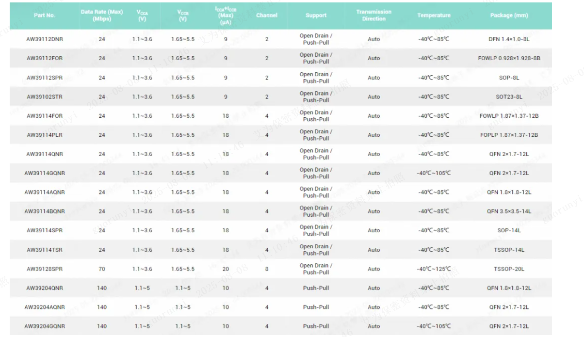
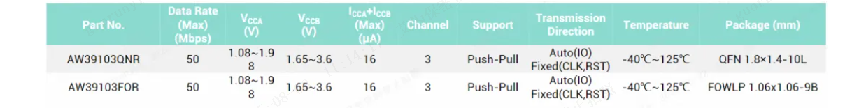
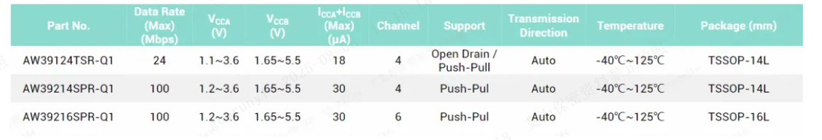
AWINIC Mass-produced Level Shift Models
Table 1 Adaptive
Direction Level Conversion Selection Table
Table 2 Direction
Controllable Level Conversion Selection Table
Table 3 Dedicated
Level Conversion Selection Table
Table 4
Automotive-grade Level Conversion Selection Table
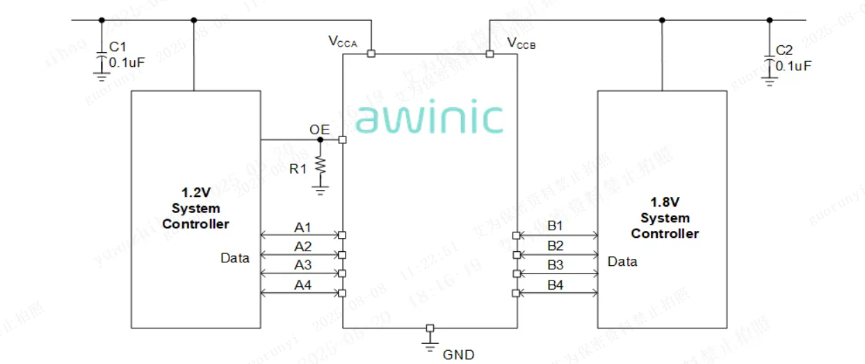
1.2V IO I²C Application Level Conversion
AWINIC provides a series of chips suitable for I²C level
conversion, including dual-channel, four-channel, and eight-channel
specifications, supporting open-drain and push-pull device access,
bidirectional signal transmission, and meeting the level adaptation condition
of VCCA ≤ VCCB.
Picture 2 Typical
Application Block Diagram of I²C Signal Level Conversion
1.2V IO SPI Application Level Conversion
1.2V SPI and other signal level conversion supports
high-speed signal push-pull applications. It is a 4-channel with automatic
direction recognition, supporting bidirectional transmission (i.e., A→B, B→A)
level conversion.
It integrates an one-shot module, which can increase the
transmission rate to over 100Mbps. Thanks to this, it is very suitable for
applications such as converting the MCLK, RESET, and SYNC signals of camera
modules from 1.2V to 1.8V, as well as converting the I2S commands issued by the
main platform to the digital PA from 1.2V to 1.8V, and general SPI and PWM
signal applications, with rich mass production experience.
Picture 3 Typical
Application Block Diagram of SPI Application Level Conversion
AWINIC's Strategic Layout for 1.2V IO Chips
With the continuous upgrading of the main chip platform's
manufacturing process, the demand for 1.2V and lower voltage IO interfaces is
increasingly prominent. As a leading domestic analog IC manufacturer, AWINIC
focuses deeply on the three core product tracks of high-performance
digital-analog mixed-signal, power management, and signal chain, and has taken
the lead in deploying support for 1.2V IO level in many devices. The following
are the technical highlights of several general-purpose products:
■AW95124FOR: 24-bit GPIO expansion (1.08V-3.6V)
■AW39103FOR: SIM card level conversion, supporting 1.2V
IO, with EMI filter and ESD protection, CSP-9B package with 0.35mm pitch
■AW86938CSR: High-voltage linear motor driver, 1.2V IO,
11V/8kB Sram, 5W driving capability, supporting AAE closed-loop control, csp
small-size package
■AW36515EFCR: Boost architecture, single-channel 2A, 1.2V
IO, I²C control, 256-level dimming flash driver
With its technical accumulation and forward-looking
layout in the analog chip field, AWINIC accurately matches the low-voltage and
low-power consumption requirements of the new generation of mobile phone main
chip platforms by optimizing device architecture and process design, providing
terminal manufacturers with more efficient and reliable chip-level solutions.