In the wave of wearable devices such as smart watches, smart bracelets, smart rings, and TWS earphones evolving towards being lighter, thinner, and smarter, the miniaturization and high efficiency of electronic components have become the core of technological breakthroughs. As a key component in power management for smart wearables, Awinic has launched the optimized ultra-miniature load switch chip AW3511XSCSR specifically for smart wearable scenarios. With features such as ultra-small packaging and ultra-light weight, it is gradually becoming the preferred solution for wearable device design.
Product Advantages
1.Ultra-Miniature Packaging: Technological Innovation Breaking Through Space Limitations
The design of smart wearable devices has always centered around "smaller, lighter, and higher integration". Awinic's previous generation of load switches adopted the small FCDFN package of 0.8mm×0.8mm×0.55mm, which greatly optimized the board layout area. The new generation of load switches utilizes Wafer-Level Chip Scale Packaging (WLCSP) technology, achieving a physical breakthrough where the package size is nearly 1:1 with the chip die. The package size is further reduced to 0.618mm×0.618mm, with a thickness of only 0.465mm. In current mainstream design schemes, this can save more than 40% of space, providing unlimited possibilities for the miniaturized design of smart wearable devices.
2.Light as a Feather: A New Breakthrough in Chip-Level Weight Reduction
Every 1 gram reduction is a qualitative leap in user experience. The single weight of the AW3511XSCSR chip is only 0.29mg, which is just 1/3 of that of conventional solutions. For complex systems that need to integrate multiple power channels (such as smart watches with multi-sensor power supply), this lightweight design can cumulatively reduce the ineffective load by 5mg, reserving valuable space for battery expansion or structural reinforcement.
While breaking through the limits of physical size, the chip still maintains advantages such as ultra-low quiescent current, low on-resistance, fast response speed, and a wide operating voltage range, truly achieving "small size with great capabilities".
Introduction to AW3511XSCSR Product
■Input voltage range: 1V ~ 5.5V
■Maximum continuous current capability: 1.5A
■On-resistance: 64mΩ@VIN=3.3V
■Ultra-low shutdown current
■Quick output discharge (QOD)
■Anti-reverse current protection (AW35113SCSR)
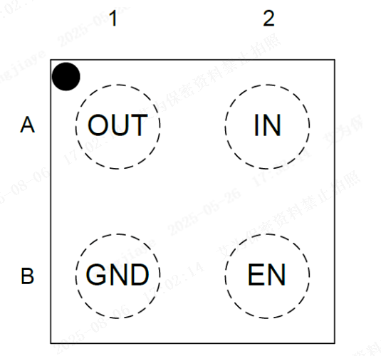
■Package:
WLCSP 0.618mm×0.618mm×0.465mm-4B
Picture 1 AW3511XSCSR Package Information
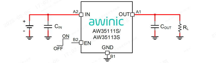
Picture 2 Typical Application Diagram of AW3511XSCSR
Picture 3 Smart watches/bracelets/rings, TWS earphones and other wearable devices
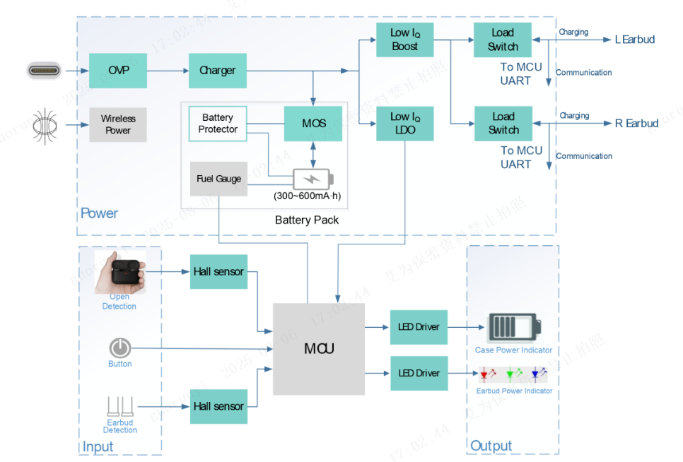
Picture 4 TWS Earphone Application Block Diagram
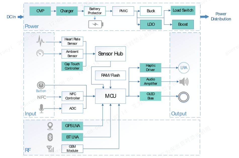
Picture 5 Smart Watch Application Block Diagram
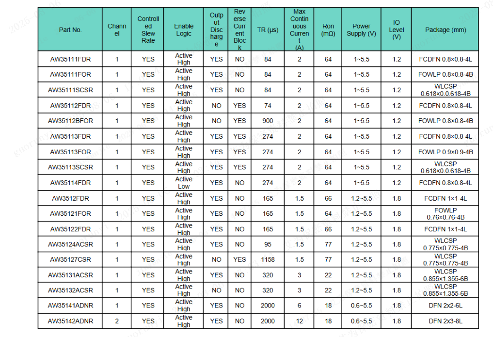
Awinic Load Switch Product Selection Table