特性
1.Operating frequency 728MHz to 960MHz
2.Noise figure(NF) =0.7dB
3.High power gain =15.5dB
4.Insertion Loss in bypass mode =3dB
5.Gain mode IIP3inb=+3.2dBm
6.Gain mode input 1dB compression point=-3dBm
7.Bypass mode input 1dB compression point= +5dBm
8.Supply voltage: 1.5V to 3.1V
9.Gain mode current 7.6mA
10.Bypass mode current <1uA
11.Input and output DC decoupled
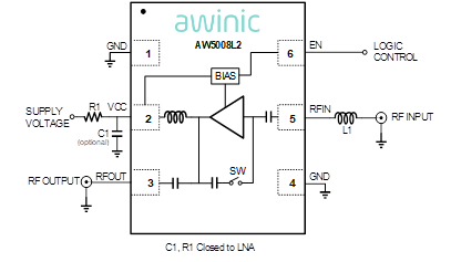
12.Requires only one input matching inductor
13.Integrated matching for the output
14.FCDFN 1.1mmX0.7mmX0.37mm -6L package
15.2kV HBM ESD protection (including RFIN and RFOUT pin)
说明
The AW5008L2 is a Low Noise Amplifier with bypass designed for LTE receiver applications. The AW5008L2 requires only one external input matching inductor, reduces assembly complexity and the PCB area, enabling a cost-effective solution.
The AW5008L2 achieves low noise figure, high linearity, high gain, over a wide range of supply voltages from 1.5V up to 3.1V. All these features make AW5008L2 an excellent choice for LTE LNA as it improves sensitivity with low noise figure and high gain, provides better immunity against jammer signals with high linearity, reduces filtering requirement of preceding stage and hence reduces the overall cost.
The AW5008L2 is available in a small lead-free, RoHS-Compliant, FCDFN 1.1mmX0.7mmX0.37 mm -6L package.