
| Load Current (mA) | DVDD: 1000 AVDD: 300 |
| Channel | 4 |
| Power Supply (Min) (V) | VIN1: 0.6 VIN2: 3 |
| Power Supply (Max) (V) | VIN1: 2 VIN2: 5.5 |
| Vout (V) | DVDD: 0.6V~1.8V AVDD: 1.2V~4.3V |
| Vdropout (mV) | DVDD: 100@0.8A AVDD: 98@0.3A |
| Iq (Typ) (μA) | 65 |
| PSRR @1KHz(dB) | DVDD: 71@10mA AVDD: 89@50mA |
| Output Noise (μVrms) | DVDD: 90@30mA AVDD: 10@30mA |
| Discharge | Programmable |
| Output options | Programmable |
| Temperature | -40℃~85℃ |
| IO Level (V) | 1.8 |
| Package (mm) | DFN 2X2-10L |
| DFN 2X2-10L |
|
类型
|
项目标题
|
语言
|
日期 | |||
|---|---|---|---|---|---|---|
| 产品设计指南 | AW37004DNR 硬件设计指南 | 中文 | 2023-03-27 | |||
| 产品设计指南 | AW37004 Software Design Guide | 中文 | 2023-04-14 | |||
| 产品手册 | DS_AW37004_EN_V1.9 | 英文 | 2025-12-07 | |||
| Checklist | CL_客户_项目_AW37004DNR_Customer_CN_V1.1 | 中文 | 2026-02-02 | |||
| 新品发布 | 艾为电子推出4通道LDO PMIC——AW37004DNR | 中文 | 2024-06-14 |
评估板
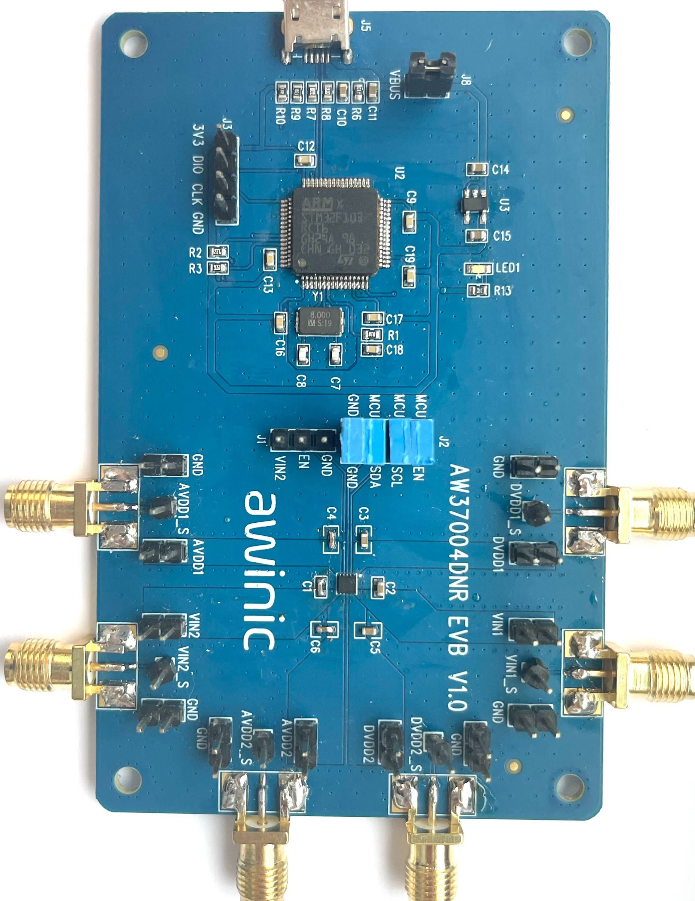
AW37004DNR EVB V1.0 — AW37004DNR EVB是一款4通道输出LDO测试板,包括2通道DVDD和2通道AVDD,芯片关键测试点均在EVB板上单独引出。
LDO AW37004DNR的EVB评估板。

应用软件和框架
AW37004_GUI — AW37004产品调试工具
AW37004 GUI是高度集成的工具,用于产品的配置和调试过程。直观的界面和人性化的操作,可以帮助客户缩短开发周期,快速的完成系统集成

评估板
AW37004DNR EVB V1.0 — AW37004DNR EVB是一款4通道输出LDO测试板,包括2通道DVDD和2通道AVDD,芯片关键测试点均在EVB板上单独引出。
LDO AW37004DNR的EVB评估板。
应用软件和框架
AW37004_GUI — AW37004产品调试工具
AW37004 GUI是高度集成的工具,用于产品的配置和调试过程。直观的界面和人性化的操作,可以帮助客户缩短开发周期,快速的完成系统集成


沪ICP备10011954号 |

沪公网安备 31011202011955号
