

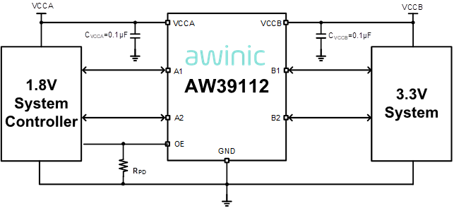
| Data Rate (Max) (Mbps) | 24 |
| VCCA (Min) (V) | 1.1 |
| VCCA (Max) (V) | 3.6 |
| VCCB (Min) (V) | 1.65 |
| VCCB (Max) (V) | 5.5 |
| ICCA+ICCB (Max) (μA) | 9 |
| Channel | 2 |
| Support | Open Drain Push-Pull |
| Temperature | -40℃~85℃ |
| Transmission Direction | Auto |
| Package (mm) | FOWLP 0.928X1.928-8B |
| FOWLP 0.928X1.928-8B |
|
タイプ
|
タイトル
|
言語
|
日付 | |||
|---|---|---|---|---|---|---|
| Datasheet | DS_AW39112DNR_FOR_EN_V1.6 | 英文 | 2025-12-19 | |||
| Checklist | CL_客户_项目_AW39112_Customer_CN_V1.0 | 中文 | 2026-02-02 | |||
| Product Design Guide | AW39112 Hardware Design Guide | 中文 | 2026-04-16 |
評価ボード
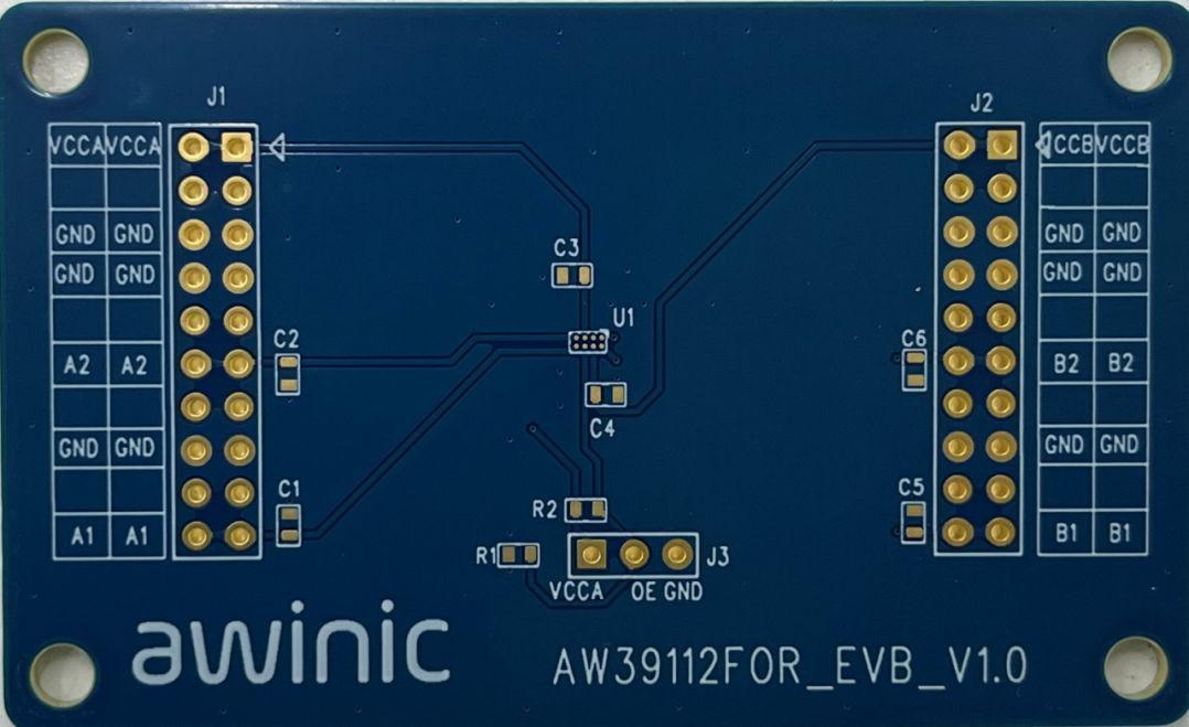
AW39112FOR_EVB_V1.0 — AW39112FOR EVB is the test board for the AW39112FOR ,awinic four-channel bidirectional voltage level translator.
This EVB is an evaluation board suitable for voltage level translator AW39112FOR

評価ボード
AW39112FOR_EVB_V1.0 — AW39112FOR EVB is the test board for the AW39112FOR ,awinic four-channel bidirectional voltage level translator.
This EVB is an evaluation board suitable for voltage level translator AW39112FOR


沪ICP备10011954号 |

沪公网安备 31011202011955号
