With the rising demand for multi-port high-speedUSBexpansion,USB3.2 Gen1leveraging its advantages in high-speed transmission and backward compatibility, has become5Gbpsthe mainstream interface fordocking stations, industrial control motherboards, and embedded devices. Based on awinic's high-performanceportAWP35817ultra-high-speed4controller chip, this article organizes a practical standardized design solution for aUSBone-to-fourHUBconfiguration from four dimensions: chip characteristics, application scenarios, key component selection, andPCBlayout, to help engineers accelerate development, avoid hazards in high-speed signal and power design, and ensure high-speed, stable device operation.USB3.2 Gen1I. Advantages of the Core Chip SolutionHubis a single-chip
protocol
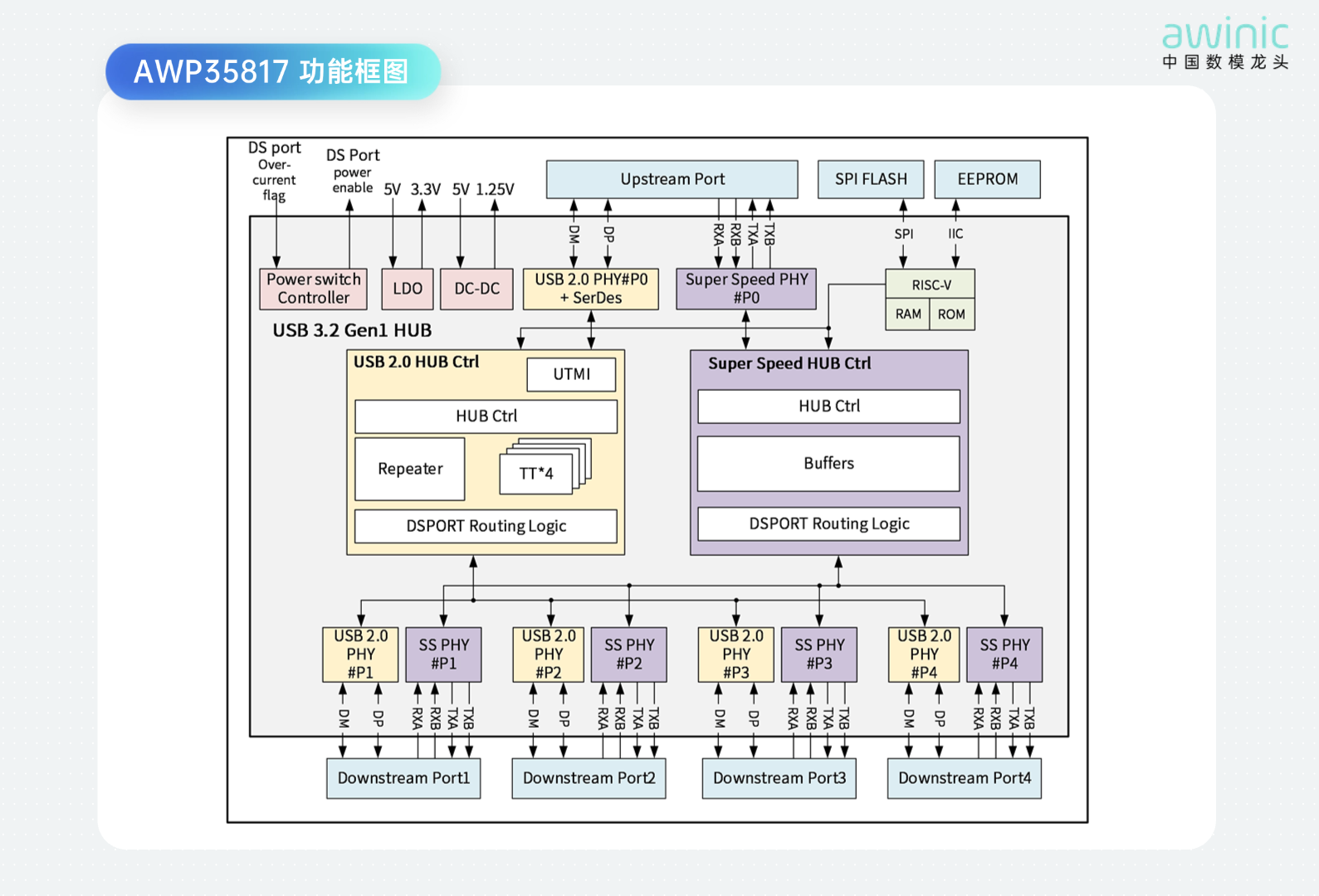
AWP35817controller solution designed specifically for high-speed multi-portUSBexpansion scenarios. Featuring high integration, simplified peripheral circuits, and strong industrial-grade stability, it enables one-stopUSB3.2 Gen1input toHUBoutputport expansion without requiring additional control chips, significantly simplifying hardware design, reducing1footprint, and meeting mass production requirements.4The chip incorporates independentUSBhigh-speedcontrollers,PCBhigh-speed
controllers, and dedicated power controllers. Equipped withUSB3.0 SSgroups andHUBgroups, it offers ample hardware resources to support concurrent high-speed transmission across multiple ports without bandwidth bottlenecks.USB2.0In terms of transmission rate compatibility, the chip provides comprehensive protocol adaptation for all ports: the upstream port supportsHUBSuperSpeed,5High-Speed, andUSB3.0 SS PHYFull-Speed modes; the downstream ports fully cover5,USB2.0 PHY,
, andUSB3.0 5GbpsLow-Speed modes, ensuring perfect compatibility with variousUSB2.0 480Mbpsperipherals such as12Mbpsflash drives, keyboards/mice, industrial sensors, and high-speed hard drives.5GbpsFurthermore, the chip supports a high-performance480Mbpsconcurrent processing mode, reasonably allocating bandwidth when multiple ports operate simultaneously to prevent overall speed reduction or lag caused by excessive occupancy on a single port. Its industrial-grade design standards enable tolerance to wide temperature ranges and complex electromagnetic environments. Compared to ordinary consumer-grade12Mbpschips,1.5Mbpsanti-interference capability, operational stability, and service life are significantly enhancedUSB, catering to both consumer and industrial product design requirements.UFigure
Functional Block DiagramMTTHUB
1 AWP35817
II. Typical Application Scenarios
Leveraging core characteristics of high integration, high compatibility, and high stability,AWP35817One-to-FourUSB3.2 Gen1 HUBThe solution adapts to hardware products across multiple fields, with core application scenarios as follows:
• Consumer Peripherals: DesktopUSBdocking stations,Type-Cmulti-function expanders, external notebookUSBsplitters, meeting the needs for simultaneous connection of multiple peripherals and high-speed data transmission in daily use
• Industrial Control Equipment: IPC motherboards, industrial embedded motherboards, industrialUSBacquisition modules, adapting to complex industrial working conditions to ensure stable communication for industrial sensors, acquisition devices, and control terminals
• Embedded Systems: Smart hardware, IoT terminals, vehicle-mounted embedded devices, security monitoring equipment, providing multi-channel standardizedUSBexpansion interfaces for embedded systems
• Computer Hardware Accessories: Desktop motherboard front-panelUSBexpansion modules, all-in-one PCUSBinterface expansion components, compensating for the shortage of native ports
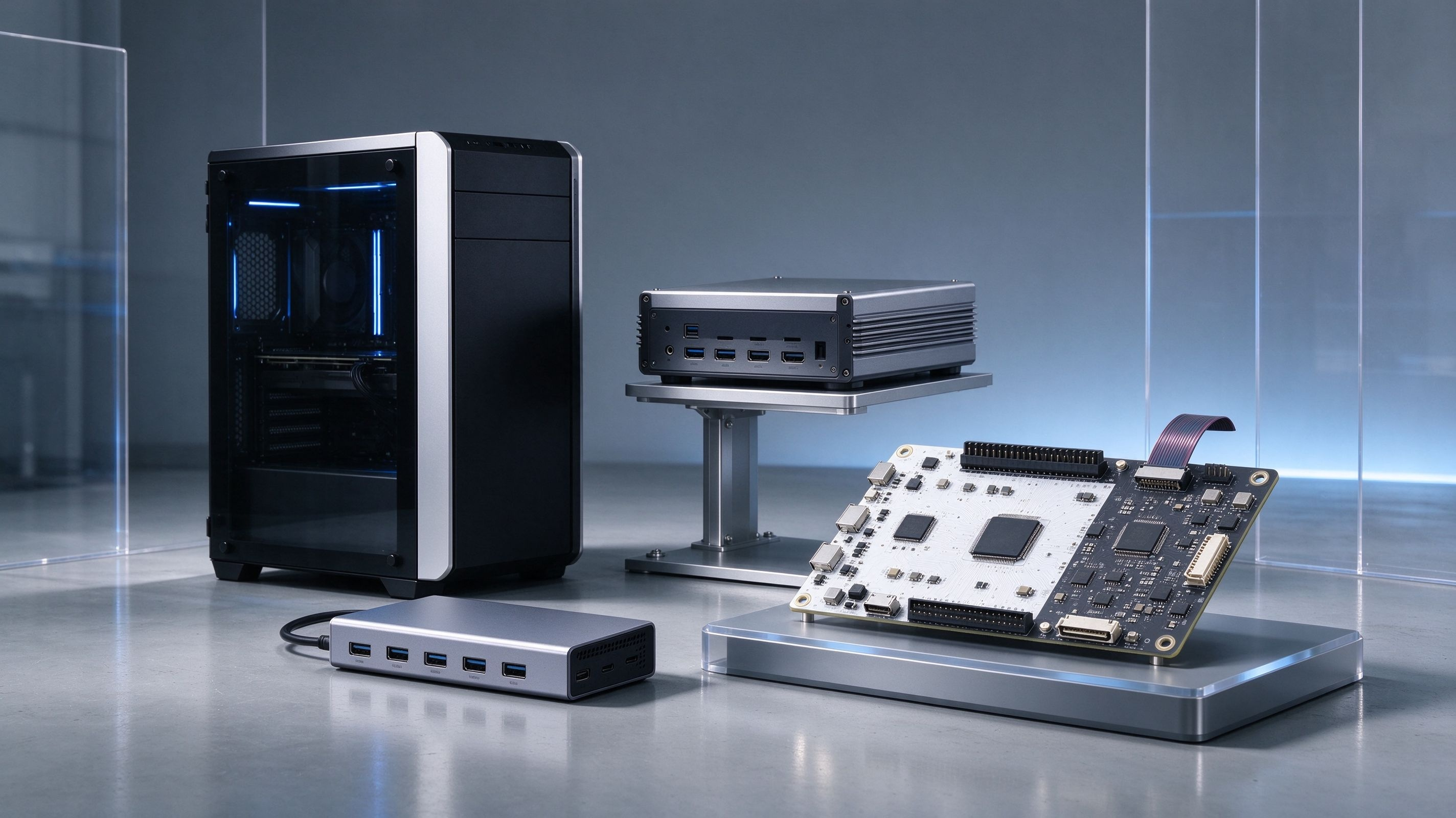
Fig. 2 Computer host,USBdocking station, IPC, and embedded system development board schematic
III. Key Component Selection and Schematic Design Specifications
The selection and layout suitability of power and passive components directly determineHUBthe power supply stability and signal purity of the awinic chip, which is the core link to avoid transmission interruptions, ripple interference, and device recognition anomalies.Based onAWP35817awinic chip hardware characteristics, standardized component selection and circuit design requirements are as follows:
3.1 1.25V DCDCPower Circuit Design
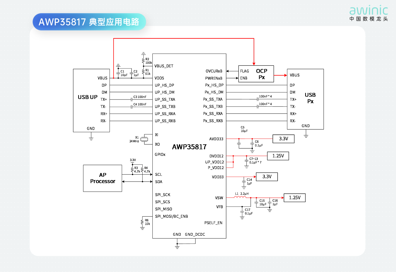
AWP35817Built-inDCDCbuck module, which can step down theVDD5pin5Vvoltage to1.25Vfor power supply; this power network has a peak operating current of approximately500mA, supplying the chip core, which is highly sensitive to power supply ripple. During design, strictly follow theproximity layout principle, and densely arrange1.25Vhigh-frequency filtering capacitors around the awinic chip0.1μFpower supply pins to filter out high-frequency noise.
DCDCModule external power device selection: Inductors with recommended inductance of2.2μHand saturation current not lower than2Aare recommended to avoid inductor saturation and abnormal supply voltage drop under high current conditions; output capacitors should adopt a combination of0.1μF~1μFsmall-value capacitors in parallel with10μFlarge-value capacitors, balancing high-frequency filtering and low-frequency voltage regulation effects. Furthermore, all capacitors and inductors must be placed close to the chip pins, with capacitors preferably arranged at the output end of the inductor to maximize suppression of power supply ripple noise. At the same time, placeFBcapacitors near the awinic chip0.1μFfeedback pins to effectively reduce feedback loop noise and ensure voltage regulation accuracy.
3.2 3.3VPower Circuit Design
The awinic chip3.3Vpower supply network has a peak current of approximately100mA;AVDD33Ground filtering capacitors must be placed near the main power supply pins ofRecommended0.1μFHigh-frequency capacitors in parallel4.7μF~10μFElectrolytic/Combination of ceramic capacitors, achieving full filtering of high and low frequency noise to ensure clean main power supply. Its built-in3.3V LDOvoltage regulation module,LDOrequires filter capacitors placed close to the chip pins at the output terminal1μFto stabilize the output voltage and prevent chip malfunction caused by voltage fluctuations.
3.3 Multi-channel input power pin design
Two independentVDD5power supply pins have clearly distinguished functions:PIN53serves as the input power supply pin for the1.25V DCDCmodule,PIN54serves as the input power supply pin for the3.3V LDOmodule.During circuit design,PIN53place the10μFinput filter capacitor nearby,PIN54place the1μFinput filter capacitor nearby; to simplify routing, the two power supply capacitors can also be combined into a1μFparallel10μFgeneral combination, uniformly arranged in theVDD5pin area, balancing filtering effectiveness with routing simplicity.
3.4 Crystal oscillator circuit design
The crystal oscillator provides the reference clock for high-speed signal transmission of the chip,its parameter accuracy directly determines theUSBtransmission stability.The design must select a24MHzstandard crystal oscillator, with frequency deviation strictly controlled within50ppm, eliminating issues such as packet loss, disconnection, and reduced transmission rates caused by clock skew. Meanwhile, the crystal oscillator must be placed close to the chip's clock pins to shorten trace length and reduce external electromagnetic interference.
3.5 USB3.0High-speed signal circuit design
USB3.0Differential transmit signal linesTXA/TXBrequire seriesAC coupling capacitorsto block DC and protect the high-speed signal link. The recommended capacitance value is0.1μF, prioritizing0402,0201small packages to reduce parasitic parameters;capacitors must be placed near theUSBport connectors symmetricallyto ensure consistency of differential link parameters and avoid signal skew and impedance mismatch.
Figure 3 AWP35817 Typical Application Circuit
IV.PCBCore Layout Specifications
USB3.2 Gen1belongs to the high-speed signal transmission protocol,5Gbpsits high bandwidth characteristics impose strict requirements onPCBtraces, impedance, grounding, and spacing. Unreasonable layout can cause signal attenuation, reflection, crosstalk, and impedance mismatch, directly leading to unstable transmission and poor compatibility. CombiningAWP35817Chip features, overviewPCBThe core layout guidelines are as follows:
4.1 Power network layout specifications
VDD5,AVDD33,DVDD12,UP_VDD12,P_VDD12,VFBFiltering capacitors for all power and feedback pins, etc., must be placed immediately adjacent to the corresponding chip pins. Long traces leading to filter failure are strictly prohibited. All power network trace widths must be no less than0.7mmto reduce line impedance, minimize voltage drop losses, and ensure sufficient power supply under high-current conditions.
4.2 High-speed differential trace length control
USB3.0High-speed signal pair trace lengths are extremely sensitive; excessive length causes signal energy attenuation and transmission reflections, compromising signal integrity. Based on standardFR4board parameters, with a board-end-7dBsignal loss as the design budget, the maximum supported trace length under typical board conditions is17.8cm, while the safe length under high-loss conditions is only14.2cm. ActualPCBlayout is recommended to be strictly controlled within14cm; precise loss parameters should be confirmed with thePCBPCB manufacturer.
At the whole-device link level,USB3.2 Gen1the maximum total insertion loss for the protocol is-20dB, with a reserved budget of-7dBfor the host side,-6dBfor the device side, andType-Cfor the public cable. Therefore, the recommended length for the complete-7dBdata cable does not exceedUSBmeters. Officially certified cables from1.8are preferred to further ensure high-speed transmission stability.USB-IFDifferential impedance and length matching design
4.3 To achieve impedance matching between transmitter and receiver,
the characteristic impedance ofUSB3.0differential signal traces must strictly match the standard value.Impedance error must be controlled within±5%toprevent signal reflection and distortion caused by impedance discontinuities.
Differential pairs must run parallel throughout their entire length with uniform and consistent spacing; sudden changes in trace spacing are prohibited. The length difference between each pair of differential signal lines must be strictly controlled within±5milto ensure synchronous signal transmission. Length optimization requires zoned processing: adjust the lengths ofUSBsignal lines andUSB2.0signal lines near theUSB3.0 RXinterface connector, and adjustUSB3.0 TXsignal line lengths near the chip pins to maximize adherence to high-speed signal transmission timing requirements.
4.4 Grounding and isolation design
USB3.0A complete, unsplit, and unslotted reference ground plane must be maintained beneath differential traces to ensure a continuous and stablesignal return path, avoiding impedance variations and signal distortion.High-speed differential signals have weak anti-interference capabilities and must maintain a safety distance of more than0.5mmfrom crystal oscillator traces, clock signals, power lines, and low-frequency control lines to prevent crosstalk interference.
4.5 Trace craftsmanship and via specifications
USB3.0Minimize corners in differential traces;90°right-angle traces are strictly prohibited. If a turn is necessary, use curved traces to reduce signal reflection and impedance fluctuation. Stubs are forbidden in high-speed signal links to avoid stray signal reflections.
Strictly control the number of vias for differential pairs; the number of vias per differential pair must not exceed2pieces, with vias symmetrically distributed. The via impedance must match the trace impedance to avoid signal loss caused by the vias. It is also recommended toUSB3.0fully ground-shield the differential traces and place return ground vias at fixed intervals to further shield against external electromagnetic interference and enhance signal anti-interference capability.
V. Solution Summary
Based onAWP35817awinic'sUSB3.2 Gen1one-to-fourHubsolution,it perfectly adapts to the high-speed port expansion needs of consumer, industrial control, and embedded scenarios, leveraging a single-chip highly integrated architecture, industrial-grade stability, and full protocol compatibility.The solution features a simplified peripheral circuit and strong mass-production viability. Through standardized component selection, power filtering design, and high-speedPCBlayout specifications, it can avoidsignal distortion, ripple interference, unstable transmission, and device compatibility anomaliesand other common issues in high-speed transmission scenarios.
This design guide covers key points throughout the schematic design, component selection, andPCBlayout processes, serving as a standardized reference basis for the R&D, debugging, and mass production ofUSB3.2 Gen1four-portHUBproducts, helping engineers rapidly deploy high-performance, high-reliabilityUSBexpansion hardware products.