AWP37503FCSR

170mA 单电感双输出电源

参考价格
  • 1-99¥5.19
  • 100-249¥4.26
  • 250-499¥3.43
  • 500-999¥2.70
  • 1000+¥2.08

产品详细信息

参数

Power Supply (Min) (V) 2.4
Power Supply (Max) (V) 5.5
Vout_POS (Min) (V) 4
Vout_POS (Max) (V) 6.5
Vout_NEG (Min) (V) -6.5
Vout_NEG (Max) (V) -4
Load Current_POS (mA) 300
Load Current_NEG (mA) 170
Temperature -40℃~85℃
IO Level (V) 1.2
Package (mm) WLCSP 1.916X1.112-15B

封装 | 引脚 | 尺寸

WLCSP 1.916X1.112-15B

特性

 2.4V 至 5.5V 输入电压  使用单电感实现双路稳压输出  正压输出电压范围: 4.0V 至 6.5V(步进 100mV)  负压输出电压范围: -6.5V 至 -4.0V(步进 100mV)  最大输出电流:170mA  卓越的综合效率 当 IOUT > 10 mA 时,η > 80% 当 IOUT > 40 mA 时,η > 85%  出色的瞬态响应与线性调整率  ±1.5% 输出电压精度  关断供电电流:1μA  欠压锁定和热关断保护  WLCSP 1.916mm×1.112mm×0.55mm-15B,0.4mm 间距封装

说明

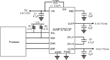
The AWP37503F is designed to support positive /negative supply for driving TFT-LCD panels mainly in smartphones and tablets. The device employs a single inductor scheme to provide a small bill-of-material and smallest PCB solution size. It integrates a step-up DC-DC converter for preceding supply. An architecture with LDO and negative charge pump (NCP) generates dual outputs at +5.4V (default) and -5.4V (default), whose voltages can be programmed via an I2C compatible interface. The device offers excellent line and load regulation performances, as well as load transient. It features an outstanding efficiency that is greater than 80% when IOUT>10mA and 85% when IOUT>40mA. With its input voltage range of 2.4V to 5.5V, it can be powered by single-cell batteries (Li-Ion, Ni-Li, Li-Polymer).

技术文档

类型
项目标题
语言
日期
产品设计指南 AWP3750XX Hardware Design Guide 中文   2025-06-26
产品手册 DS_AWP37503F_CN_V1.1 中文   2026-08-17
产品手册 DS_AWP37503F_EN_V1.1 英文   2026-08-17
可靠性报告 Reliability Qualification Report For AWP37503FCSR 英文   2026-09-15

设计和开发

如需其他信息或资源,请查看下方列表,点击标题即可进入详情页面。