AW39102STR

2-Bit Bidirectional Voltage-Level Translator for Open-Drain and Push-Pull Applications

参考价格
  • 1-99¥3.08
  • 100-249¥2.52
  • 250-499¥2.03
  • 500-999¥1.60
  • 1000+¥1.23

产品详细信息

参数

Data Rate (Max) (Mbps) 24
VCCA (Min) (V) 1.1
VCCA (Max) (V) 3.6
VCCB (Min) (V) 1.65
VCCB (Max) (V) 5.5
ICCA+ICCB (Max) (μA) 9
Channel 2
Support Open Drain<br>Push-Pull
Temperature -40℃~85℃
Transmission Direction Auto
Package (mm) SOT23-8L

封装 | 引脚 | 尺寸

SOT23-8L

特性

• Voltage Level Translator Without Direction-Control Signal
• Maximum Data Rates
- 24Mbps (Push Pull)
- 2Mbps (Open Drain)
• Power Supply Range:
- A Port and VCCA: 1.1V to 3.6 V
- B Port and VCCB: 1.65 V to 5.5 V
- VCCA ≤ VCCB
• Pull Up Resistors are Integrated in A Port and B Port
• No Power-Supply Sequencing Required: Either VCCA or VCCB Can be Ramped First
• Support Ultra-Low Power Consumption Mode with OE Pin is Low Voltage Level
• Latch -Up Performance Exceeds ±200mA Under JESD78E Standard
• WBSOT23-8L Package

说明

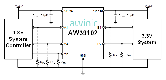
AW39102 is a 2-bit high-performance voltage-level translator without direction control signal, which is a non-inverting converter and can be used to convert digital signal with mixed-voltage systems. It needs two separate power supply rails, with the A ports tracks the VCCA ranging from 1.1 V to 3.6 V, and the B ports tracks the VCCB ranging from 1.65 V to 5.5 V. This makes the chip has capabilities of support both lower and higher logic signal levels translation between any of the 1.2V, 1.8 V, 2.5 V, 3.3 V, and 5 V voltage nodes.
The OE input circuit is supplied by VCCA. Meanwhile, OE is recommended to be tied to GND through an external pull-down resistor to ensure all I/O to be pulled to the supply voltage. No power supply sequencing requirements means either VCCA in VCCB can be powered up first, and OE should be enabled after both VCCA and VCCB are established.

技术文档

类型
项目标题
语言
日期
产品设计指南 AW39102 硬件设计指南 中文   2023-05-17
产品手册 DS_AW39102_EN_V1.1 英文   2023-06-06

设计和开发

如需其他信息或资源,请查看下方列表,点击标题即可进入详情页面。