AW35111FDR

2A Ultra-small Load Switch with Slew Rate Control

参考价格
  • 1-99¥1.35
  • 100-249¥1.10
  • 250-499¥0.89
  • 500-999¥0.70
  • 1000+¥0.54

产品详细信息

参数

Channel 1
Controlled Slew Rate YES
Enable Logic Active High
Output Discharge YES
Reverse Current Block NO
TR (μs) 84
Max Continuous Current (A) 2
Ron (mΩ) 64
Power Supply (Min) (V) 1
Power Supply (Max) (V) 5.5
Temperature -40℃~85℃
IO Level (V) 1.8
Package (mm) FCDFN 0.8X0.8-4L

封装 | 引脚 | 尺寸

FCDFN 0.8X0.8-4L

特性

● Integrated P-channel MOSFET load switch ● Input voltage: 1V to 5.5V ● 2A maximum continuous switch current ● Switch on-resistance(typ.): Rdson=52mΩ at VIN=5.5V Rdson=57mΩ at VIN=4.2V Rdson=64mΩ at VIN=3.3V Rdson=76mΩ at VIN=2.5V Rdson=100mΩ at VIN=1.8V Rdson=164mΩ at VIN=1.2V Rdson=230mΩ at VIN=1V ● Controlled slew rate to limit inrush currents ● Ultra low shutdown current ● Internal EN pull-down/up resistor ● Quick Output Discharge(QOD) for AW35111/ AW35113/AW35114 ● Full time Reverse Current Protection (RCP) for AW35112/AW35112B/AW35113 ● FCDFN 0.8mm×0.8mm-4L package FOWLP 0.8mm×0.8mm-4B package FOWLP 0.9mm×0.9mm-4B package

说明

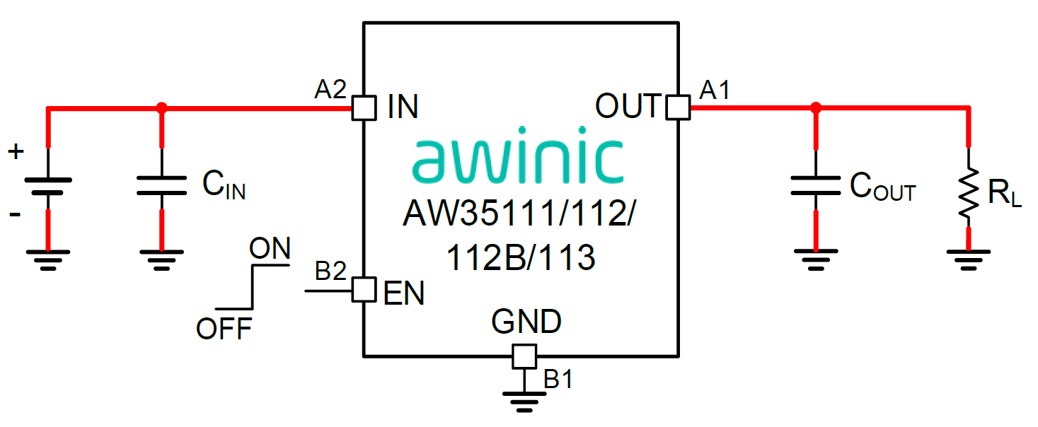
The AW3511X family load switch integrates a 64mΩ (typ.) P-channel MOSFET, which can operate over a wide input range of 1V to 5.5V. The AW3511X features output slew rate control, limiting inrush currents during turn-on to protect downstream devices.
In addition, AW35111/ AW35113 have QOD function which can prevent the output from floating when the switch is disabled.
There is a Reverse Current Protection(RCP) function for AW35112/AW35112B/AW35113 when VOUT is 33mV(typ.) greater than VIN, which can prevent the current to flowing through the P-FET in the body diode. There is no output discharge resistor for AW35112 and AW35112B.

技术文档

类型
项目标题
语言
日期
产品设计指南 AW3511X 硬件设计指南 中文   2024-03-25
产品手册 DS_AW3511X_EN_V1.8 英文   2026-07-23
新品发布 【新品发布】超小超薄+纳安级低功耗!艾为AW3511x负载开关解锁便携终端电源轻薄续航新方案 中文   2026-07-14

设计和开发

如需其他信息或资源,请查看下方列表,点击标题即可进入详情页面。