AW12022FLR

0.1-6GHz DPDT Antenna Cross Switch

参考价格
  • 1-99¥2.69
  • 100-249¥2.21
  • 250-499¥1.78
  • 500-999¥1.40
  • 1000+¥1.08

产品详细信息

参数

Frequency (GHz) 0.1~6
Switch Feature DPDT Antenna
Control Interface GPIO
VDD (Min) (V) 1.65
VDD (Max) (V) 3.3
VIO (Min) (V) /
VIO (Max) (V) /
P0.1dB (dBm) 39
IL (Min) (dB) 0.27
IL (Max) (dB) 0.57
ISO (Max) (dB) 33
ISO (Min) (dB) 17
Temperature -40℃~85℃
Package (mm) FCLGA 1.5X1.1-10L

封装 | 引脚 | 尺寸

FCLGA 1.5X1.1-10L

特性

• Broadband frequency range: 0.1 to 6.0GHz
• Wide VDD range: 1.65V to 3.3V
• GPIO interface for 1.0V to VDD positive control voltage
• Low insertion loss: 0.35dB typical @ 2.7GHz
• Max input RF power of 39dBm
• Excellent linearity and harmonic performance
• No DC blocking capacitors in typical application
• Small FCLGA (1.1mm x 1.5mm x 0.47 mm -10L) package

说明

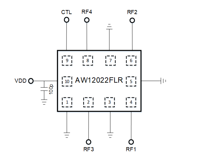
The AW12022FLR is a Silicon-On-Insulator(SOI) DPDT switch with low insertion loss and high Isolation. It can be used to support band switching and mode switching for cellular 4G/5G, data cards and tablets.
The symmetrical design of internal ports makes it convenient for PCB routing and adjustment of receiving and transmitting signals. The band/mode switching is realized by the GPIO pin as referenced in the chip block diagram and the control logic. The chip allows power-supply voltages from 1.65V to 3.3V and the positive control voltages from 0.5*VDD to VDD.
The AW12022FLR is provided in a compact FCLGA 1.1mm x 1.5mm x 0.47mm -10L package

技术文档

类型
项目标题
语言
日期
产品手册 DS_AW12022_6GHz_DPDT_EN_V1.3 英文   2023-06-06
技术帖 【技术贴】I²C通信故障深度解析:艾为全链路经验指南 中文   2025-10-09
技术帖 【技术贴】超低功耗黑科技!艾为AW86320 高压液冷驱动IC,散热新宠诞生 中文   2025-06-20
技术帖 【技术帖】80后、90后童年回忆升级!艾为游戏掌机方案助力时代新宠 中文   2024-08-12

设计和开发

如需其他信息或资源,请查看下方列表,点击标题即可进入详情页面。