

| Channel | 1 |
| Controlled Slew Rate | YES |
| Enable Logic | Active High |
| Output Discharge | NO |
| Reverse Current Block | YES |
| TR (μs) | 74 |
| Max Continuous Current (A) | 2 |
| Ron (mΩ) | 64 |
| Power Supply (Min) (V) | 1 |
| Power Supply (Max) (V) | 5.5 |
| Temperature | -40℃~85℃ |
| IO Level (V) | 1.8 |
| Package (mm) | FCDFN 0.8X0.8-4L |
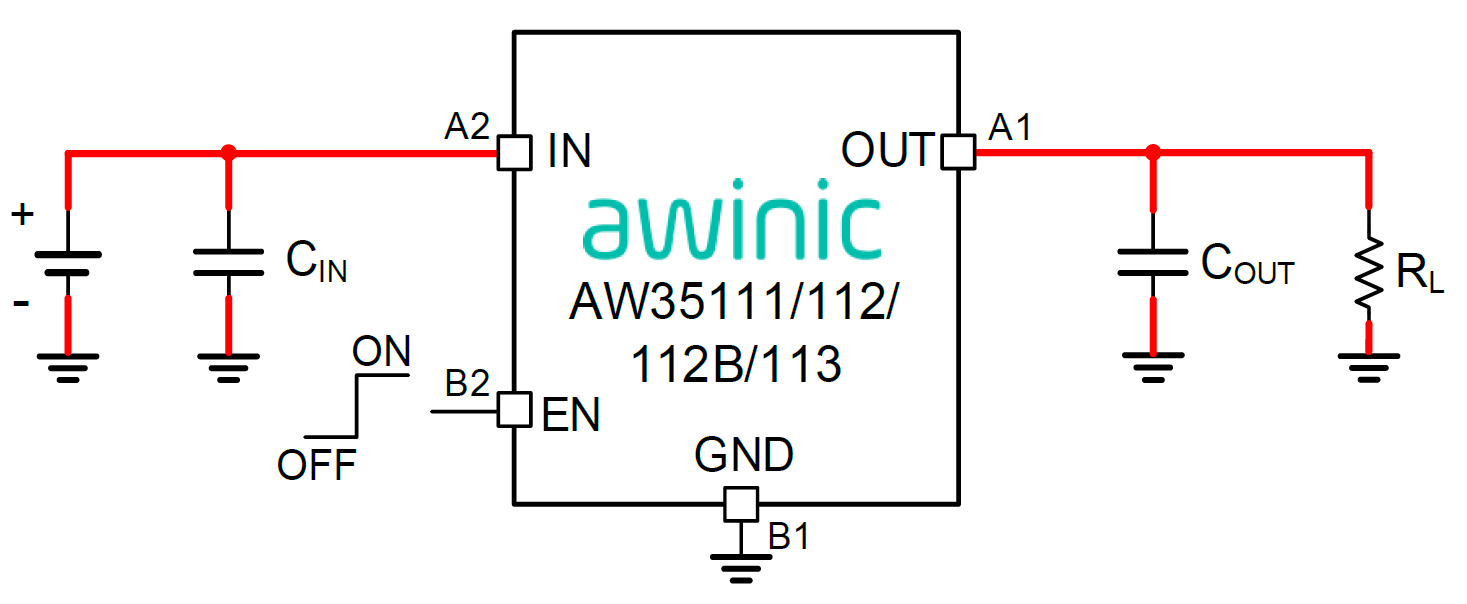
| FCDFN 0.8X0.8-4L |
|
유형
|
제목
|
언어
|
날짜 | |||
|---|---|---|---|---|---|---|
| Product Design Guide | AW3511X 硬件设计指南 | 中文 | 2024-03-25 | |||
| Datasheet | DS_AW3511X_EN_V1.8 | 英文 | 2026-07-23 |
평가 보드
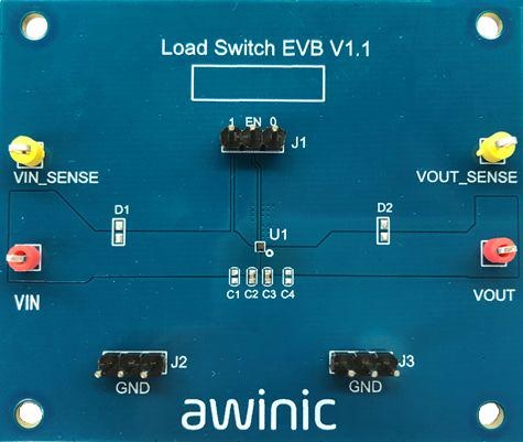
Load Switch EVB V1.1 — Load Switch EVB is the evaluation board of load switch series AW3511X. The key test points of the chip are led out separately on the test board for convenient testing.
EVB evaluation board for load switch series AW3511X

평가 보드
Load Switch EVB V1.1 — Load Switch EVB is the evaluation board of load switch series AW3511X. The key test points of the chip are led out separately on the test board for convenient testing.
EVB evaluation board for load switch series AW3511X


沪ICP备10011954号 |

沪公网安备 31011202011955号
