

| Power Supply (Min) (V) | 2.4 |
| Power Supply (Max) (V) | 5 |
| Vout_POS (Min) (V) | 4 |
| Vout_POS (Max) (V) | 6.5 |
| Vout_NEG (Min) (V) | -6.5 |
| Vout_NEG (Max) (V) | -4 |
| Load Current_POS (mA) | 300 |
| Load Current_NEG (mA) | 120 |
| Temperature | -40℃~85℃ |
| IO Level (V) | 1.2 |
| Package (mm) | QFN 3X3-16L |
| QFN 3X3-16L |
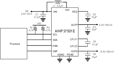
|
タイプ
|
タイトル
|
言語
|
日付 | |||
|---|---|---|---|---|---|---|
| Product Design Guide | AW3750X_Software_Design_Guide | 中文 | 2025-08-12 | |||
| Product Design Guide | AW3750X_Software_Design_Guide | 英文 | 2025-08-12 | |||
| Product Design Guide | AWP3750XX Hardware Design Guide | 中文 | 2026-02-03 | |||
| Datasheet | DS_AWP37501EQNR_EN_V1.0 | 英文 | 2026-02-10 | |||
| Reliability Report | Reliability Qualification Report For AWP37501EQNR | 英文 | 2026-05-19 |

APPLICATION SOFTWARE&FRAMEWORK
AW3750X_GUI — Integrated debugging tool for AW3750X product
AW3750X product integration debugging tool is used for product configuration debugging. The interface is intuitive and easy to operate, helping users quickly complete product Functional verification
APPLICATION SOFTWARE&FRAMEWORK
AW3750X_GUI — Integrated debugging tool for AW3750X product
AW3750X product integration debugging tool is used for product configuration debugging. The interface is intuitive and easy to operate, helping users quickly complete product Functional verification


沪ICP备10011954号 |

沪公网安备 31011202011955号
