

| Control Interface | GPIO |
| Current Limit (Typ) (A) | 1.4 |
| Load Current (Max) (A) | 0.6 |
| Vout (Min) (V) | 4.5 |
| Vout (Max) (V) | 4.5 |
| Output Type | Fixed |
| Temperature | -40℃~85℃ |
| Special Function | Down Mode PSM Mode PFM Mode PWM Mode Pass through Mode |
| Package (mm) | DFN 2X2-6L |
| DFN 2X2-6L |
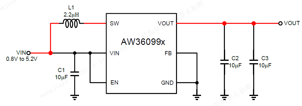
|
タイプ
|
タイトル
|
言語
|
日付 | |||
|---|---|---|---|---|---|---|
| Product Design Guide | AW36099x Hardware Design Guide | 中文 | 2023-05-18 | |||
| Datasheet | DS_AW36099_EN_V2.0 | 英文 | 2025-07-18 | |||
| Technical articles | 【技术贴】DC/DC的FB引脚作用详解 | 中文 | 2024-07-05 |
評価ボード
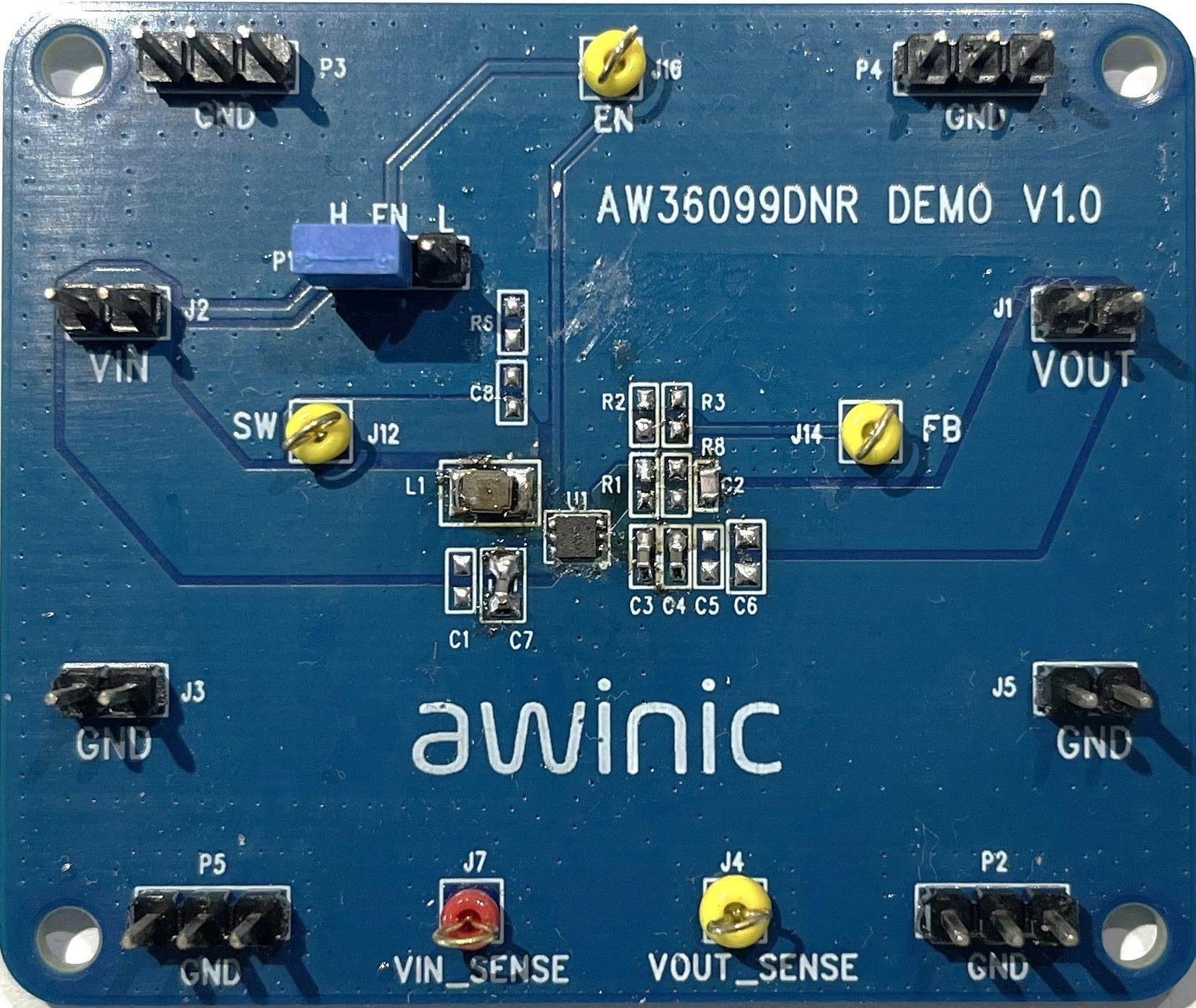
AW36099DNR DEMO V1.0 — AW36099xDNR EVB is the evaluation board of low Iq Boost circuit AW36099xDNR. The key test points of the chip are led out separately on the test board for convenient testing.
Evaluation board for low Iq Boost circuit AW36099xDNR.

評価ボード
AW36099DNR DEMO V1.0 — AW36099xDNR EVB is the evaluation board of low Iq Boost circuit AW36099xDNR. The key test points of the chip are led out separately on the test board for convenient testing.
Evaluation board for low Iq Boost circuit AW36099xDNR.


沪ICP备10011954号 |

沪公网安备 31011202011955号
