

1. Introduction: Receive Sensitivity——Cellular Communication's“Hearing”Key
In cellular (Cellular) communication,receive sensitivity (Receiver Sensitivity)is one of the key metrics measuring whether a device can operate normally inweak signal environments“blind spots”
In cellular (Cellular) communication systems, with an increasing number of frequency bands and the widespread application ofCA/MIMO/ENDCtechnology, noise and interference in the receive path have become increasingly complex. In the receive path, theLow Noise Amplifier (LNA)often serves as thefirst active component“extract”useful signals from noise.
2. Principle:LNAHow awinic Helps
To understandLNAwhy awinic can improve receive sensitivity, one must first understand what“factors”theoretically affect receive sensitivity. Receive sensitivity is theminimum signal strengththat a receiver can detect at an acceptable bit error rate, which can be expressed by the following formula:

Here, -174 dBm/Hz is the thermal noise floor at room temperature, NF is the total noise figure of the receive chain, SNR_min is the minimum signal-to-noise ratio required for demodulation, and B is the signal bandwidth. In RF front-end receive circuits, SNR_min is mainly determined by the signal modulation scheme, while B is determined by the actual communication bandwidth. Since the modulation scheme and bandwidth are defined by the communication protocol and are independent of the RF front-end circuit design, reducing NF is the most direct way to improve sensitivity.
According to the cascaded noise formula(calculated using linear values), it can be concluded that the total noise of a multi-stage amplifier is primarily determined by the noise and gain of the first stage. In other words, as long as the first stageLNAhas sufficiently low noise and high gain, subsequent circuit stages (such asSAW,Transceiveretc.) introduced noise will be“suppressed”, having a negligible impact on the overall system noise.

In common receiver systems,LNAis typicallythe first active component, andTransceivertends to have relatively high noise. Therefore, selecting alow-noise, high-gainLNAcan almost completely suppress the impact of subsequent stages on the totalNF, making the overall systemNFapproachLNAtheNFvalue of the component itself, thereby improving reception sensitivity. In practical applications, placing theeLNAas close as possible to the RF front-end (antenna side) and systematically optimizing matching to reduce front-end insertion loss can typically reduce the total linkNFby approximately3dB.
3. LTE LNAFor selection, which parameters should be considered?
For a qualifiedLTE LNA, mainly consider these indicators:
Noise Figure (NF): Directly determines the amount of noise introduced by theLNAitself; lowerNFis better, and is key to improving sensitivity.
Gain (Gain): Used to amplify useful signals while simultaneously“suppressing”downstream noise. However, higher gain is not always better; excessive gain leads to reduced linearity and easily causes saturation distortion under strong signal conditions. From the cascaded noise formula, it can be derived that when gain increases to a certain level, further increases yield minimal improvement to the system'sNF. Therefore, commonLTE LNAgain is around18dB; higher gain provides negligible improvement to the systemNF.
1dBCompression Point (P1dB): When communication devices are near base stations receiving strong signals, theLNAeasily enters thesaturation region, leading to gain compression and generatingharmonic distortion, reducing sensitivity
Third-Order Intercept Point (IP3): Multi-carrier/Multi-band coexistence scenarios,Such asCarrier Aggregation (CA)or simultaneous reception of signals with different standards,LNAnon-linearity will causeintermodulation products (IMD). If these fall within the operating band, they cannot be filtered out; in this case, theIP3specification is particularly critical.
Bypass Mode (Bypass Mode): When the mobile phone is very close to the base station, the received signal is strong. At this time, if theLNAstill operates in high-gain mode, the input signal will far exceed its linear range, causing the amplifier to enter saturation.Bypass Modeallows theLNAto be“bypassed when necessary.”——The signal does not pass through the active amplification stage but is transmitted directly to the subsequent circuit via alow-loss bypass.
Power Consumption (ICC): For mobile devices such as smartphones and tablets, low power consumption is a strict requirement. LNA The operating current of awinic is typically between a few milliamperes and ten-plus milliamperes,By passwhile the quiescent current in 1μAmode needs to be controlled within.
Operating Frequency Range (Frequency Range): LNAawinic'sDatasheetdatasheet will recommend frequency bands, but in some application scenarios, the recommended bands and target bands do not match perfectly. In such cases, externalmatching components can be used to match theLCawinic device to the target band. For example,LNAcan be matched toGNSS LNA, andN255can be configured as a band-MB LTE LNABypass ModeGNSS LNA.
4. Product Example: awinicLTE LNASolution
awinic has been deeply engaged in the RF field for over a decade, with RF products focusing primarily onLNAandRF Switchdirections. In terms ofLTEfrequency bands, awinic has launched a product matrix covering both low and high bands completely. Among them,AWR15008HDNRandAW5008HGDNRare representative products designed for different frequency band requirements.
AWR15008HDNR:
Focusing onLTE HBandBDSfrequency bands2300MHz~2690MHz
Simple external matching, easy debugging: Only one inductor needs to be connected in series at the input
Noise figure as low as0.72dB
Gain up to18.5dB
Built-inBypassFunction:Bypass ModeCurrent less than1μA
Package:DFN 1.1mm×0.7mm–6L
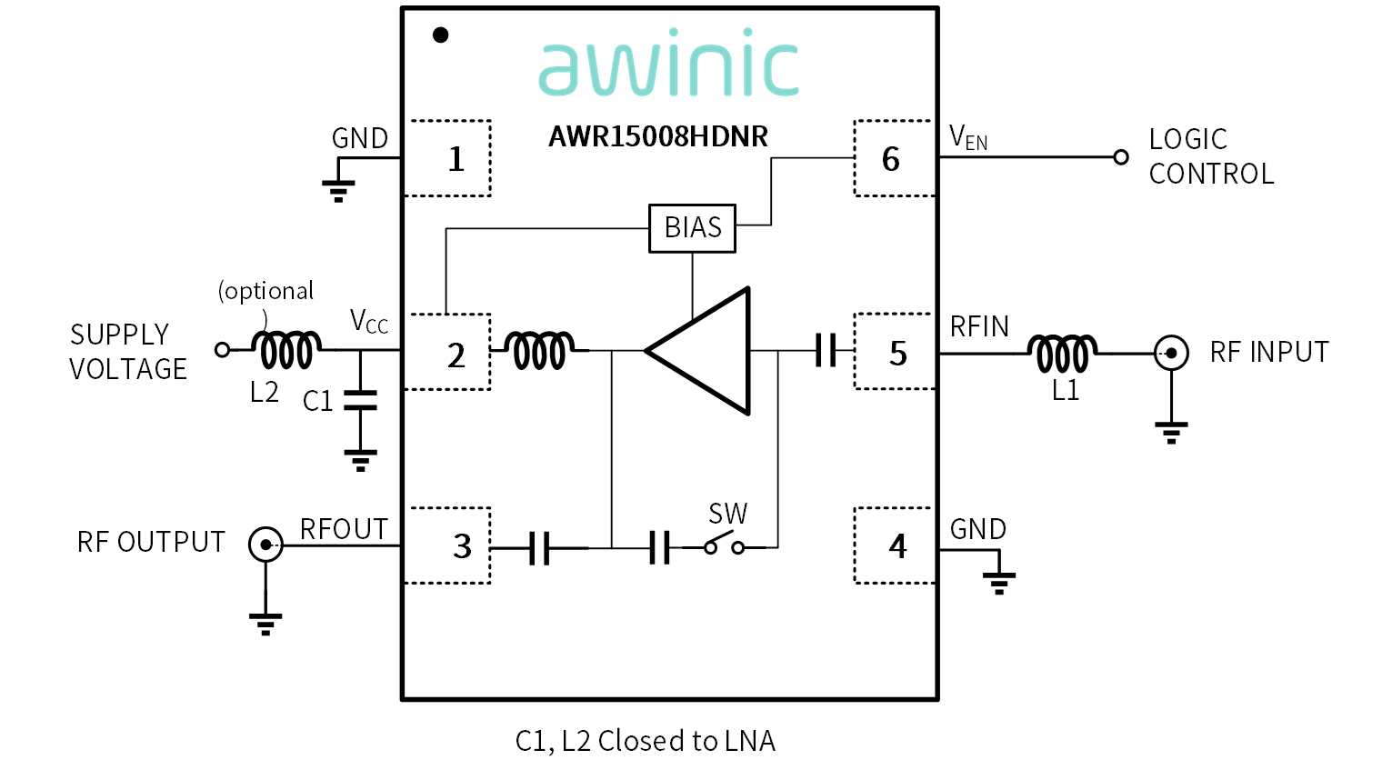
Figure1: AWR15008HDNR Typical Application Diagram
AW5008HGDNR:
SupportsLTE MHB,NTNMainstream bands 1425MHz~2200MHz and 2300MHz~2690MHz
Simple peripheral matching for easy debugging: Only requires a single inductor in series at the input
NF:0.55dB@1425MHz~1560MHz,0.6 dB @1800MHz~2200MHz,0.75 dB @2300MHz~2690MHz
Gain up to20.5dB
Built-inBypassFunction:Bypass ModeCurrent less than1μA
Package:DFN 1.1mm×0.7mm–6L
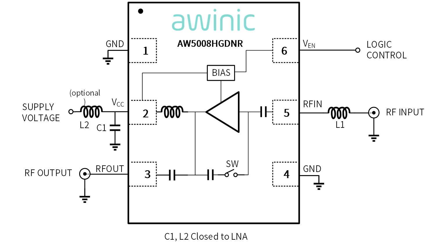
Figure2: AW5008HGDNR Typical Application Diagram
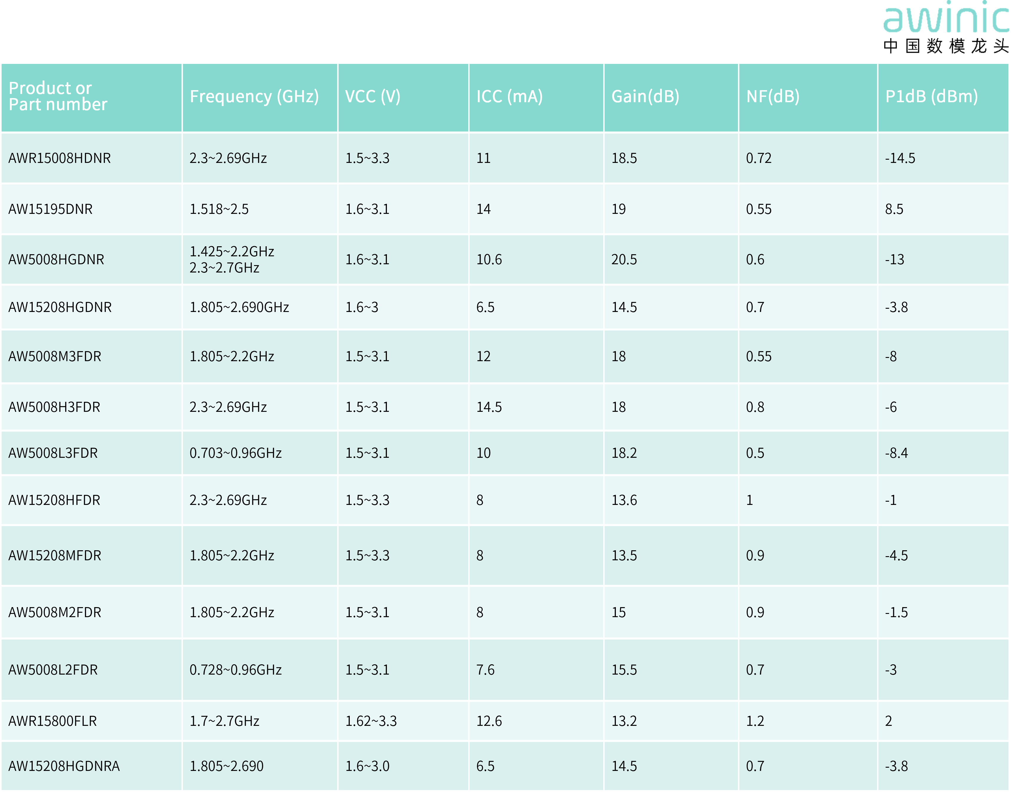
In addition, awinic also providesCovering700 MHzto2690 MHzA completeLNAProduct matrix,NFFrom0.5 dBto1.2 dBVarying, with gain flexibly selectable between13 dBto21 dB. Coverage of different operating voltages and temperatures enables compatibility with more application scenarios.
5. Conclusion
LNAJust like the“Goalkeeper”of the receive chain, creating clean working space for subsequent circuits with low noise and high gain. Many awinic products have achieved a good balance amongLow noise, high gain, and low power consumption. Whether for flagship smartphones or IoT modules, suitable combinations can be found. In today's world where5Gis gradually becoming ubiquitous,LTEwill still exist for the long term, and an excellentLNAremains an indispensable“Unsung hero”for enhancing user experience.


沪ICP备10011954号 |

沪公网安备 31011202011955号
