

Most people judge a TFT-LCD screen by visible specs like resolution and brightness, rarely paying attention to the thumbnail‑sized bias chip on the back of the panel. The ability of such a screen to precisely control the electric field at every pixel relies on the “thin‑film transistor” (TFT) inside the liquid‑crystal panel – each pixel has its own tiny switch. The bias chip acts as the “voltage heart” of this system: it must supply a stable reference voltage to the source driver for accurate grayscale signal output, deliver enough VGH high‑level voltage to quickly turn on the TFT switches row by row so that pixels can charge and discharge properly, and generate a negative VGL voltage to completely turn off the TFT switches and prevent pixel charge leakage. A deviation in any one of these voltages can cause image sticking, stepped grayscale jumps, or even a black screen in severe cases.
In some small‑to‑medium‑size products (e.g., smartphones and tablets), a dedicated bias chip is used to generate positive and negative voltages VSP/VSN (±4 V to ±6.5 V) as the core power supply for the source driver. AWINIC already has a mature product solution for this – the AW3750X series.
In the application scenario of TFT‑LCD screens, here we share a driver IC that can generate the key voltages AVDD, VGH, VGL, and VCOM, along with its working principles.
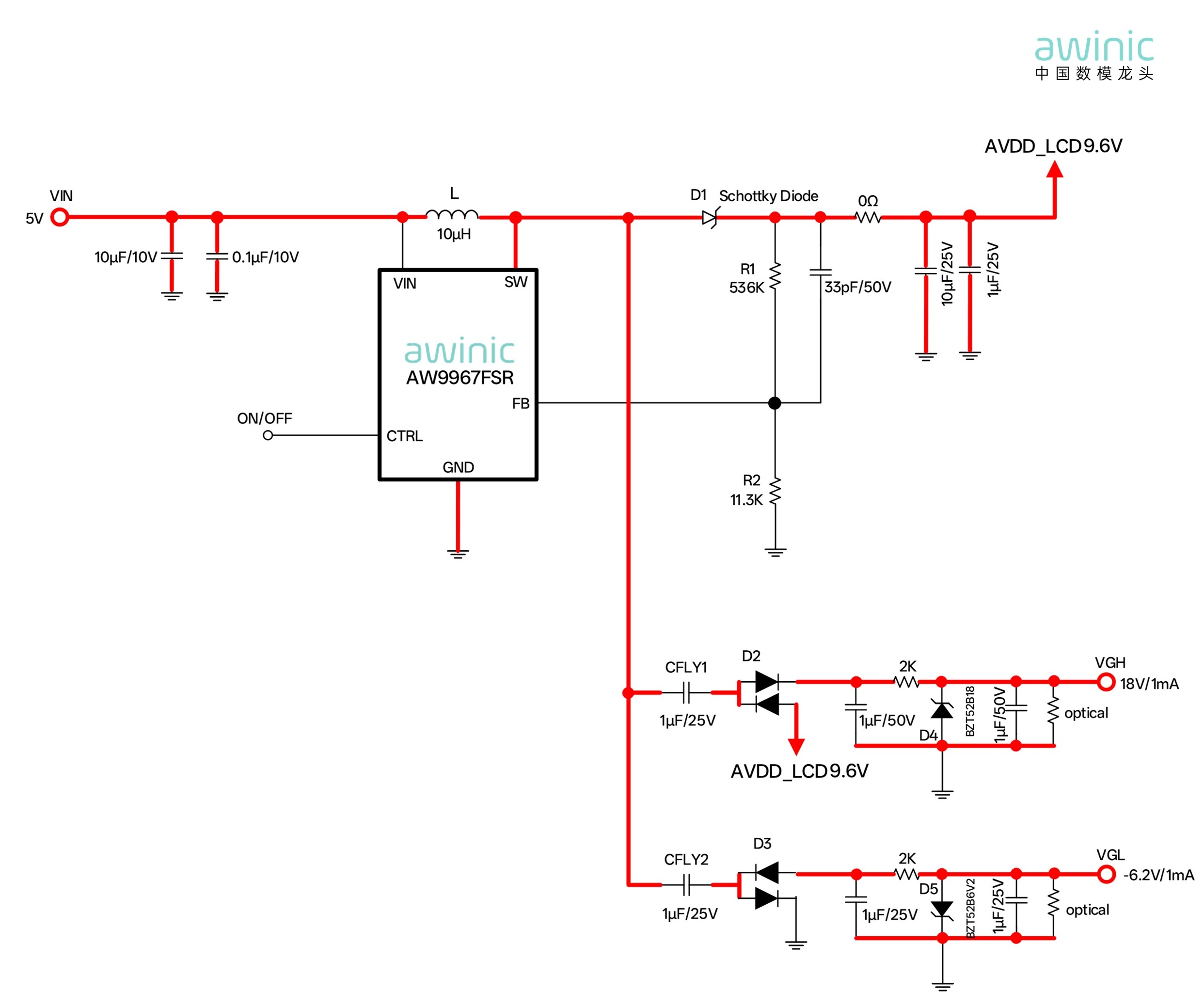
Figure 1. Typical application circuit for TFT‑LCD screen bias using the AW9967FSR
Key voltages for TFT‑LCD screens:
AVDD: Analog module power supply, typically generated by a boost converter, with current usually around 10–20 mA.
VGH: Positive voltage that controls the turn‑on of the TFT gate electrode. When a row of the LCD display is scanned, the gate line of that row is driven to VGH, turning on all TFTs in that row so that the data voltage can be written into the pixel capacitor. The current is typically a few mA, not exceeding 10 mA.
VGL: Negative voltage that controls the turn‑off of the TFT gate electrode. After the LCD scanning finishes, the gate line voltage is pulled down to VGL to ensure the TFT is completely turned off, keeping the pixel capacitor charge stable until the next frame refresh. The current is typically a few mA, not exceeding 10 mA.
VCOM: Common electrode voltage for the liquid crystal, also serving as the reference voltage for LCD driving.
The following table lists the voltage requirements of a typical TFT panel (note that different panels may have different specifications):
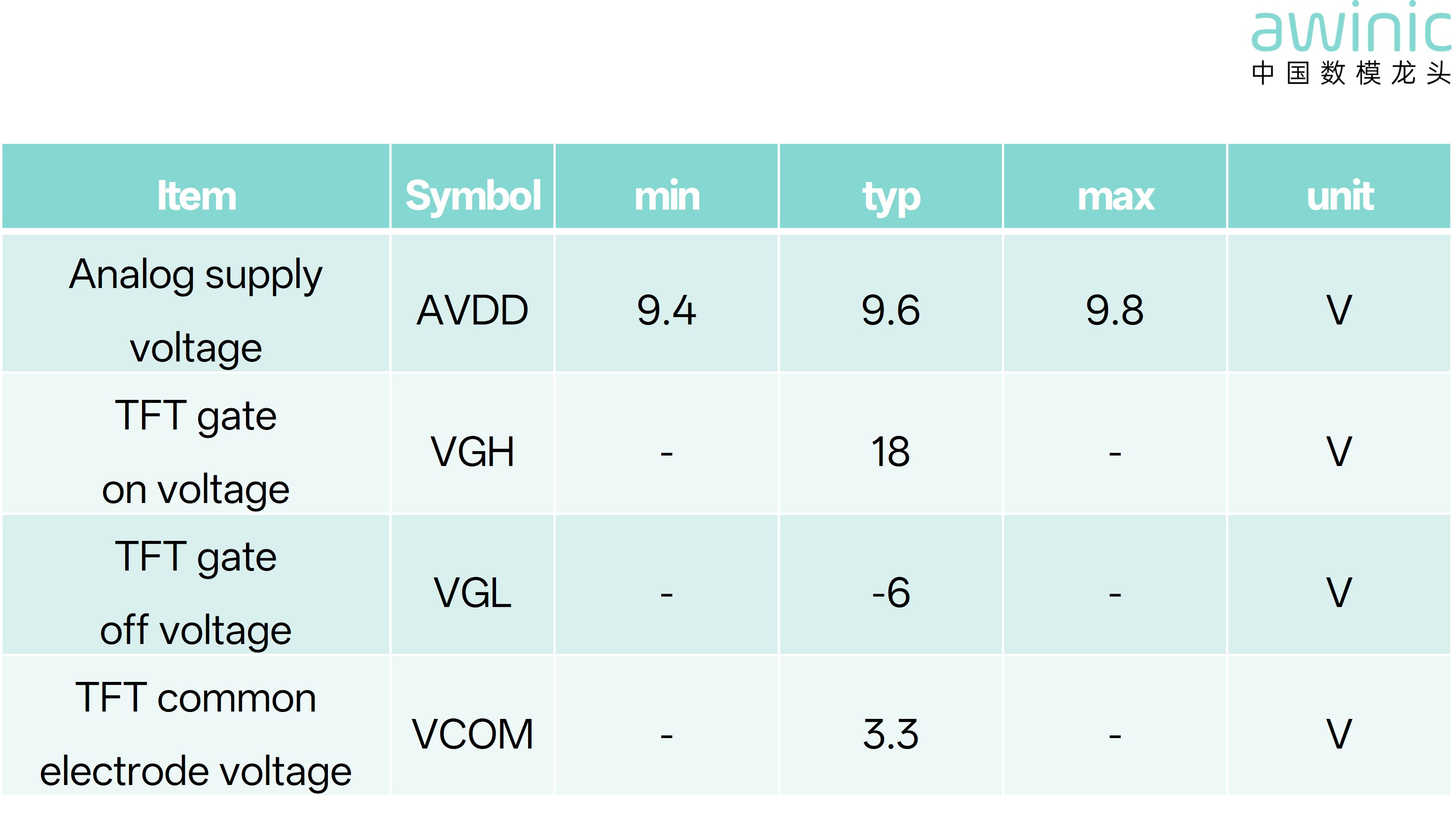
Table 1. Voltage requirements of a typical TFT panel
Basic principles for generating each voltage:
AVDD: This is a synchronous boost topology formed by inductor L, Schottky diode D1, output capacitors, and the IC. For detailed boost principles, refer to AWINIC’s [Technical Article] Analysis of Buck‑Boost Fundamentals.
VGH – Positive charge pump circuit (voltage doubler):
When the internal power MOSFET is on, the SW pin voltage is 0 V. The storage inductor L is charged through the internal switch, and the flying capacitor CFLY1 is also charged through the internal switch, with its left plate negative and right plate positive, and a voltage difference across it of approximately 9.6 V − Vd2 (diode forward drop). When the internal power MOSFET turns off, the SW node voltage rises to about 9.6 V + Vd1. Since the voltage across the capacitor cannot change abruptly, the left side of CFLY1 becomes 9.6 V + Vd1, and its right side becomes approximately 19.2 V + Vd1 − Vd2. This voltage then passes through diode D2 and a current‑limiting resistor, and is clamped by a Zener diode, so the final output voltage is clamped to 18 V.
VGL – Negative charge pump circuit (inverting voltage doubler):
When the internal power MOSFET is off, the SW node voltage is about 9.6 V + Vd1. The flying capacitor CFLY2 is charged through diode D3 to ground, and the voltage across CFLY2 rises to about 9.6 V + Vd1 − Vd3. When the internal power MOSFET turns on, the left side of CFLY2 is pulled to 0 V. Since CFLY2 was charged to nearly 9.6 V in the previous step and the capacitor voltage cannot change abruptly, the right side of CFLY2 becomes −9.6 V. This voltage then passes through diode D3 and a current‑limiting resistor, and is clamped by a Zener diode, so the final output voltage is clamped to −6 V.
VCOM: Mainly used to maintain voltage stability and compensate for leakage current. The current is generally small, from a few mA to around 10 mA. VCOM can be obtained directly from the AVDD voltage via a resistor divider.
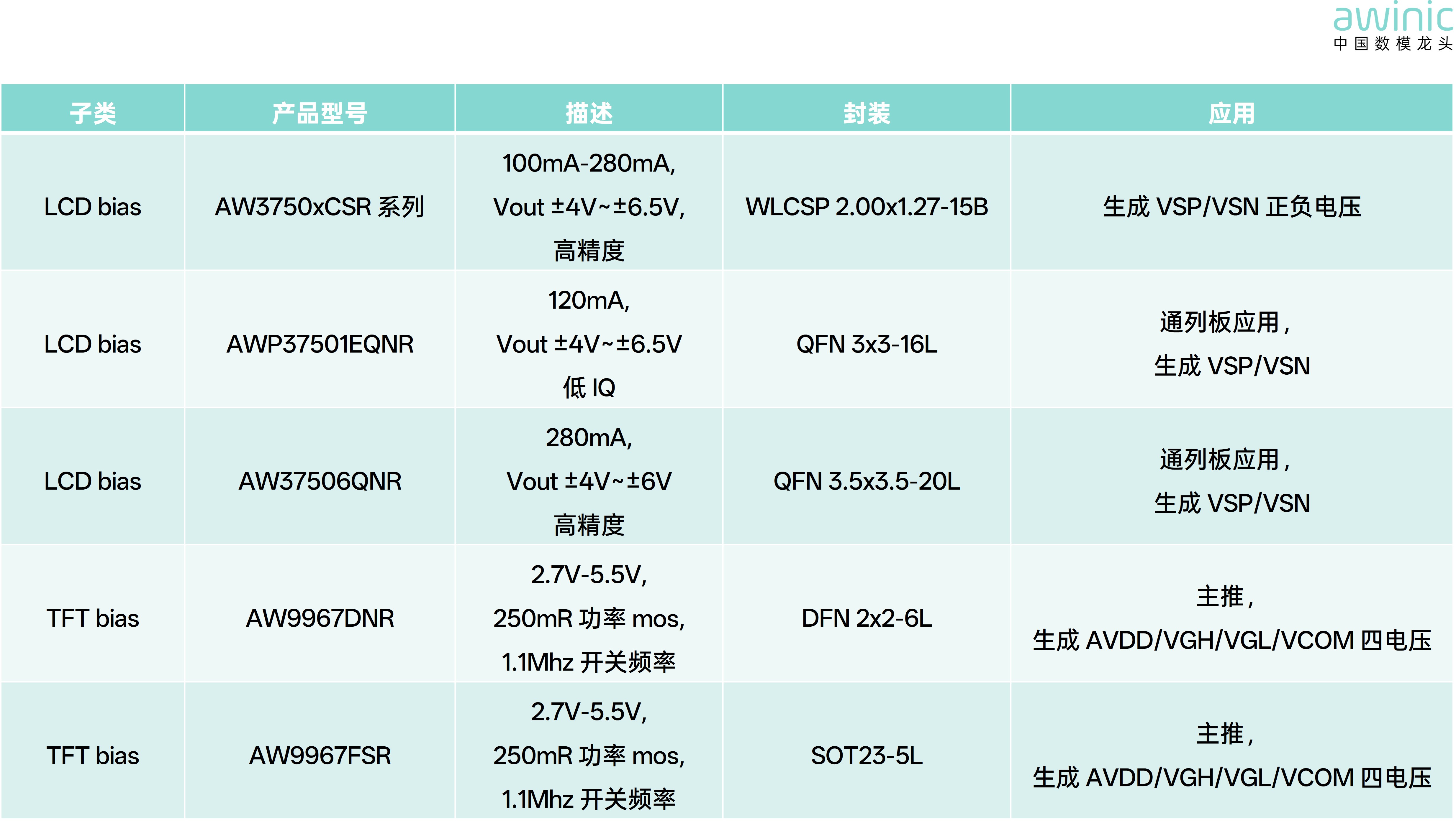
Table 2. AWINIC product selection list for screen bias related solutions
AWINIC, a leading domestic company in mixed‑signal, power management, and signal‑chain ICs, has years of deep experience in analog and mixed‑signal chips. Targeting typical screen‑display applications, AWINIC has developed highly reliable, low‑power, highly integrated, and multi‑package solutions for backlight drivers, bias ICs, and OLED power ICs, fully meeting the needs of various screen‑driver applications.


沪ICP备10011954号 |

沪公网安备 31011202011955号
